Thin film ceramic design rules are tighter than thick film rules by roughly an order of magnitude — trace/space minimums of 10–25 µm versus 100–150 µm — because the metallization is sputtered and patterned photolithographically rather than screen-printed. Getting those fine features to survive etching, trimming, and assembly requires specific substrate, metal stack, and layout choices made before the first mask is drawn.
Key Takeaways
- Minimum trace and space for production thin film on polished alumina is typically 10–25 µm, depending on metal stack thickness and substrate flatness.
- Substrate surface roughness (Ra) must stay below 25 nm for reliable sub-50 µm features; 96% alumina is usually too rough without lapping.
- Thin film NiCr or TaN resistors can be trimmed to ±0.1% or better with laser trimming, but layout must allow adequate trim path clearance.
- Total metal stack thickness rarely exceeds 3–5 µm before plating; thicker conductors require additive copper plating.
- CTE mismatch between substrate and solder pads drives reliability in thermal cycling — plan pad geometry accordingly.
Substrate Selection for Thin Film
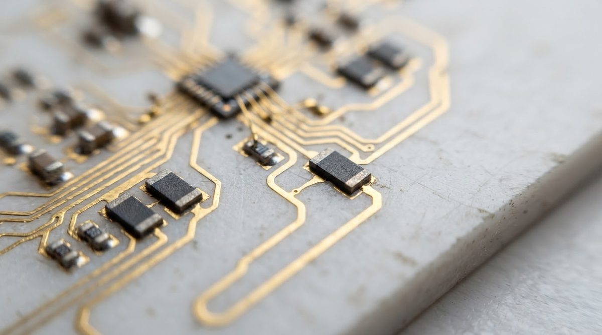
The substrate surface is the foundation of every thin film design rule. Sputtered films conform to the substrate topography, so surface defects reproduce directly into the metallization. A scratch or pit wider than the trace pitch creates an open or short.
99.6% alumina (Al₂O₃) is the default substrate for thin film work. After lapping and polishing, it reaches Ra values of 5–15 nm, well within the range needed for 10–25 µm features. 96% alumina can be used for coarser designs (≥50 µm trace/space), but its as-fired surface roughness of 0.3–0.6 µm Ra requires polishing to get below 25 nm. Aluminum nitride (AlN) is chosen when thermal conductivity matters — 170–200 W/mK versus 24–28 W/mK for 96% Al₂O₃ — but AlN substrates cost roughly 3–5× more and require careful surface preparation. For detailed thermal trade-offs on AlN, see the AlN thermal design guide.
| Parameter | 99.6% Al₂O₃ | 96% Al₂O₃ (polished) | AlN | Unit |
|---|---|---|---|---|
| Surface roughness (Ra), polished | 5–15 | 15–40 | 10–25 | nm |
| Thermal conductivity (20 °C) | 28–35 | 24–28 | 170–200 | W/mK |
| Dielectric constant (1 MHz) | 9.7–9.9 | 9.2–9.6 | 8.5–9.0 | — |
| CTE (25–300 °C) | 7.2–7.4 | 6.5–7.2 | 4.4–4.7 | ppm/°C |
| Flexural strength (ASTM C1161) | 380–450 | 300–380 | 300–350 | MPa |
Typical values for commercially available material, for comparison only. Confirm against the datasheet for your specific grade.
Metal Stack and Minimum Feature Sizes
A standard thin film metal stack on alumina starts with a sputtered adhesion layer (typically 20–50 nm TiW or Cr), followed by a barrier/resistor layer (NiCr or TaN, 10–100 nm), and a conductor layer (Au or Cu, 0.5–3 µm sputtered, optionally plated thicker). The total sputtered thickness before plating is usually 1–3 µm.
Minimum trace and space scale with total metal thickness and etch method. For a 1 µm gold conductor on polished 99.6% alumina, 10–15 µm lines and spaces are achievable with ion-beam or wet-chemical etching and a stepper-exposed photoresist. For thicker conductors (3–5 µm plated copper), the practical floor rises to 20–25 µm trace/space because of plating uniformity limits. If your design needs conductors thicker than 5 µm, review copper plating capabilities and tolerances to confirm what is feasible on ceramic.
Worked Example: Minimum Trace Width for a 50 Ω Microstrip
Assume a 254 µm thick 99.6% alumina substrate (εr = 9.8) with a sputtered gold conductor 1.5 µm thick. Using standard microstrip equations (per IPC-2141), the trace width for 50 Ω is approximately 240 µm — well above the minimum feature size. Thin film’s advantage here is not narrower traces but tighter width tolerance: ±2 µm versus ±25 µm for thick film screen printing, which translates to impedance control of roughly ±0.5 Ω instead of ±3–5 Ω. For coplanar waveguide designs where gap dimensions are critical, the coplanar waveguide ceramic design guide covers gap-specific rules.
Thin Film Resistor Design Rules
Embedded thin film resistors are one of the primary reasons to choose thin film over thick film. NiCr sputtered at 50–200 Ω/sq (depending on film thickness) and TaN at 50–300 Ω/sq give designers access to precision resistors without discrete components.
Critical layout rules for thin film resistors:
- Aspect ratio. Keep the resistor length-to-width ratio between 0.5:1 and 10:1. Ratios above 10:1 increase sensitivity to width variation and worsen TCR matching.
- Trim path clearance. Laser trim cuts (typically 10–30 µm kerf width) need at least 50 µm clearance from adjacent conductors and other resistors. Design the resistor body wide enough to accommodate an L-cut or serpentine trim without cutting into the termination.
- Termination overlap. The conductor must overlap the resistor film by at least 50 µm on each end to ensure low-resistance contact. Misalignment tolerance eats into this overlap, so 75–100 µm is safer for multi-mask processes.
- Minimum resistor dimension. Below 100 µm in either direction, sheet resistance variation across the film dominates the tolerance. Practical minimum body size for ±1% as-deposited tolerance is 100 × 100 µm; for ±0.1% after laser trimming, 200 × 200 µm or larger.
Via and Interconnect Rules
Thin film ceramics are typically single-layer or two-layer circuits. Through-substrate vias on thin film ceramics are laser-drilled (typically 50–150 µm diameter) and metallized by sputtering plus plating. The minimum via diameter depends on substrate thickness; an aspect ratio of 1:1 to 3:1 (depth:diameter) is standard. For designs requiring filled vias, consult the ceramic via filling process to understand fill material options and planarity limits.
Pad-to-via registration on thin film is ±5–10 µm (photolithographic alignment), far better than the ±25–50 µm typical of thick film. This allows smaller capture pads — via diameter plus 20–30 µm annular ring on each side is sufficient.
When Not to Use Thin Film Ceramic
Thin film is the wrong process when any of the following apply:
- Features are coarser than 75 µm. Thick film ceramic processes handle 100–150 µm trace/space at lower cost per unit area, with simpler tooling.
- High current conductors are needed. If you require copper thicker than 20 µm across the full circuit, DBC or thick film with plating is more practical.
- Budget is the primary constraint. Thin film mask sets, sputtering, and photolithography cost 2–5× more than thick film screen printing for equivalent substrate area. For volumes above 10,000 units with relaxed tolerances, thick film almost always wins on cost.
- The substrate is not polished. Running thin film on an as-fired 96% alumina surface will produce unreliable fine features. Either add polishing cost or switch processes.
Process-Specific Tolerances Summary
| Parameter | Thin Film (typical) | Thick Film (typical) | Unit | Condition / Source |
|---|---|---|---|---|
| Min trace width | 10–25 | 100–150 | µm | On polished 99.6% Al₂O₃; per Kyocera thin film design guide |
| Min space | 10–25 | 100–150 | µm | Same |
| Trace width tolerance | ±2–5 | ±20–30 | µm | Photolithography vs. screen print |
| Resistor as-deposited tolerance | ±1–5 | ±10–20 | % | NiCr/TaN sputtered vs. RuO₂ printed |
| Resistor trimmed tolerance | ±0.1–0.5 | ±0.5–1 | % | Laser trim, per Vishay thin film app note |
| Layer-to-layer registration | ±5–10 | ±25–50 | µm | Stepper alignment vs. screen alignment |
| Conductor thickness (sputtered) | 0.5–3 | 8–15 (printed) | µm | Before plating |
Typical values for commercially available material, for comparison only. Confirm against the datasheet for your specific grade.
Frequently Asked Questions
What substrate surface roughness do I need for thin film?
For features below 50 µm, the substrate Ra should be under 25 nm. Polished 99.6% alumina routinely achieves 5–15 nm Ra. Unpolished 96% alumina (Ra 300–600 nm) is unsuitable without lapping.
Can I mix thin film resistors and thick film conductors on the same substrate?
Yes, but it adds process steps and cost. The thin film resistor layer is sputtered and patterned first, then thick film conductors are screen-printed and fired. The firing temperature (~850 °C for Au thick film) must not degrade the thin film resistor’s TCR. This hybrid approach is used in some military and space circuits where both precision resistors and high-current conductors are needed.
How does thin film ceramic compare to thin film on silicon?
Silicon offers smoother surfaces and well-established semiconductor fab processes, but alumina provides better high-frequency performance (lower dielectric loss at GHz frequencies), higher operating temperatures (no junction limits), and better thermal shock resistance. Ceramic is preferred for RF hybrids, power resistor networks, and sensors operating above 200 °C.
What is the maximum operating temperature for a thin film ceramic circuit?
The ceramic substrate itself withstands well above 1000 °C, but the thin film metallization limits the operating range. Gold-based stacks are stable to 300–350 °C in air. NiCr resistors begin drifting above 200–250 °C depending on passivation. Solder joints, not the thin film, are usually the first component to limit temperature in an assembled circuit.
Do I need a passivation layer over thin film traces?
For most applications, yes. A sputtered SiO₂ or Si₃N₄ passivation layer (200–500 nm) protects thin film resistors from humidity and contamination drift. Conductors that will be wire-bonded or soldered are masked open during passivation deposition.
Next Step
If your design is past schematic and you are ready to set up layer rules, the thin film ceramic layout guidelines cover Gerber preparation, keepout zones, and panelization specifics. To get a quote on a thin film ceramic board, submit your files through the instant quote form and an engineer will review your design rules within one business day.