A multilayer ceramic PCB is a monolithic substrate formed by laminating and co-firing multiple layers of ceramic green tape, each carrying screen-printed conductor patterns. LTCC (low-temperature co-fired ceramic) fires at 850–900 °C and accepts silver or gold conductors; HTCC (high-temperature co-fired ceramic) fires at 1 500–1 600 °C and uses tungsten or molybdenum metallisation. Both processes produce hermetic, dimensionally stable boards with buried signal lines, ground planes, and thermal vias—capabilities that post-fired single-layer ceramics cannot match.
Key Takeaways
- LTCC supports 4 to 50+ layers with silver or gold conductors; HTCC typically reaches 10–40 layers with refractory metals.
- Fired shrinkage is 12–16 % in X-Y for standard LTCC tapes (per Ferro A6M datasheet), making tight dimensional control the central design challenge.
- Minimum via diameter in production LTCC is 75–100 µm; HTCC vias are typically ≥ 150 µm due to the stiffer green tape.
- Multilayer ceramic adds 3–10× the cost of a single-layer DPC or DBC board—justified only when buried routing, hermeticity, or RF performance demands it.
- Single-layer or two-layer ceramic processes (DPC, thick film) handle most power-electronics and LED thermal applications more cost-effectively.
How Multilayer Ceramic PCBs Are Made
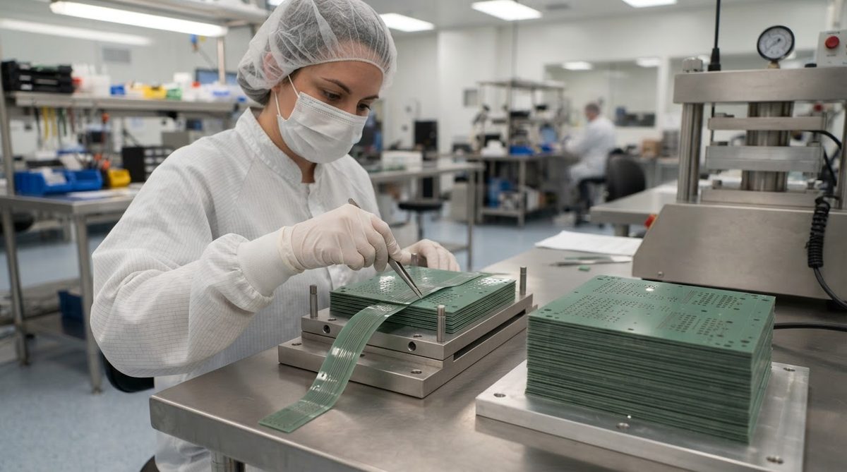
The process starts with casting a ceramic slurry (alumina, glass-ceramic, or aluminium nitride powder in an organic binder) into thin green tape, typically 50–250 µm per layer. Each sheet is laser- or mechanically punched for vias, then screen-printed with conductor paste. Layers are stacked in a precise registration fixture, laminated under heat and pressure (70–80 °C, 20–25 MPa for LTCC per DuPont 951 processing guidelines), and co-fired in a single kiln cycle. The organic binder burns out below 500 °C; sintering fuses the ceramic and metal into one solid body.
Because every layer shrinks during firing, the manufacturer must compensate conductor artwork by the inverse of the shrinkage factor. A tape with 12.7 % X-Y shrinkage needs artwork scaled to roughly 114.5 % of final dimensions. Zero-shrinkage LTCC techniques—where sacrificial constraining layers hold X-Y dimensions—can reduce in-plane shrinkage to under 0.1 %, but they add process cost and limit layer count. For a full walkthrough of ceramic fabrication steps, see how ceramic PCBs are manufactured.
LTCC vs HTCC for Multilayer Builds
| Parameter | LTCC | HTCC | Unit / Condition | Source |
|---|---|---|---|---|
| Firing temperature | 850–900 | 1 500–1 600 | °C | Ferro / Kyocera datasheets |
| Typical layer count | 4–50+ | 10–40 | layers | Industry practice |
| Conductor metals | Ag, Au, AgPd | W, Mo, MoMn | — | DuPont 951 / CoorsTek ADS-996 |
| Conductor resistivity | 2–5 | 8–15 | mΩ/sq (fired, 10 µm thick) | DuPont / Kyocera |
| Dielectric constant (εr) | 5.7–7.8 | 9.0–10.0 (96 % Al₂O₃) | at 1 MHz, 25 °C | Ferro A6M / CoorsTek ADS-96R |
| Thermal conductivity | 2–4 (glass-ceramic) | 18–28 (96 % Al₂O₃) | W/m·K at 25 °C | Ferro / CoorsTek |
| Min via diameter | 75–100 | 150–200 | µm | Production capability |
| X-Y shrinkage tolerance | ±0.2–0.5 % | ±0.3–0.5 % | of nominal | Manufacturer specs |
Typical values for commercially available material, for comparison only. Confirm against the datasheet for your specific grade.
LTCC wins on conductor loss, fine features, and layer count. HTCC wins on thermal conductivity and mechanical strength. For RF modules, LTCC’s lower εr and silver conductors reduce insertion loss. For power packages that must dissipate heat through the substrate, HTCC alumina or aluminium nitride is the better base material. Understanding ceramic thermal management trade-offs helps you decide which path fits your thermal budget.
Design Rules for Multilayer Ceramic Stacks
Layer thickness and count
Each fired dielectric layer is typically 50–200 µm thick. Thinner layers improve via aspect ratios and reduce total substrate height but are harder to handle during lamination. A 20-layer LTCC stack with 100 µm layers yields a finished substrate roughly 2 mm thick—comparable to a standard FR-4 board. Beyond 30 layers, warpage management and via registration become the limiting factors.
Via design
Stacked vias (column vias running through every layer) provide the lowest inductance path for grounding and thermal conduction. Staggered vias save routing space but add inductance. For RF ground returns below 10 GHz, keep via pitch under λ/20 to prevent cavity resonance—at 10 GHz in LTCC (εr ≈ 7), that means via spacing ≤ 1.1 mm.
Shrinkage compensation—a worked example
Suppose your LTCC tape (Ferro A6M) has a nominal X-Y shrinkage of 15.4 %. You need a finished pad-to-pad distance of 10.000 mm. The pre-fired artwork dimension is:
10.000 mm ÷ (1 − 0.154) = 10.000 ÷ 0.846 = 11.820 mm
With a shrinkage tolerance of ±0.3 %, the fired dimension lands between 9.970 mm and 10.030 mm. If your design requires ±10 µm positional accuracy, standard LTCC cannot meet it without post-fire laser trimming or zero-shrinkage processing.
Embedded passives
LTCC allows screen-printing resistors (10 Ω/sq to 1 MΩ/sq) and capacitors (using high-K dielectric layers, up to ~50 pF/mm²) inside the stack. This eliminates surface-mount parts and shortens interconnects—valuable in RF front-end modules where parasitic inductance degrades filter performance.
Where Multilayer Ceramic Excels
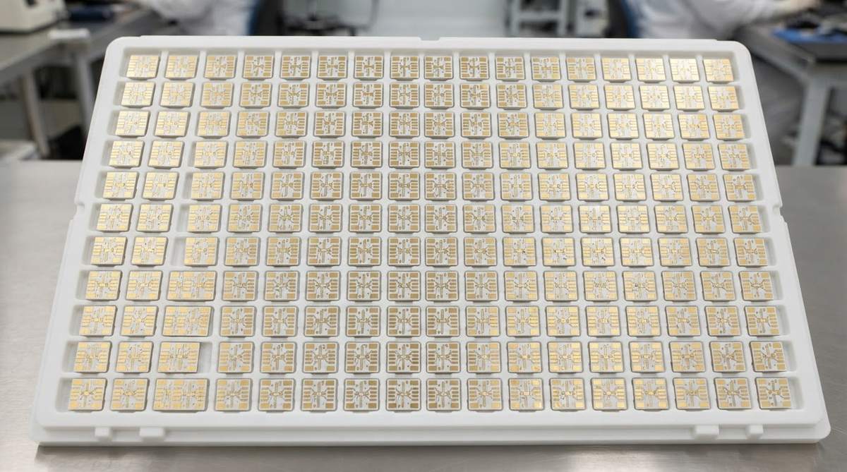
RF and microwave modules (1–77 GHz). Stripline and coplanar waveguide structures buried in a controlled-εr dielectric deliver repeatable impedance. LTCC modules are standard in automotive radar (77 GHz), satellite downconverters, and military T/R modules.
Hermetic packages. A co-fired ceramic body with brazed seal rings provides true hermeticity (leak rate < 1 × 10⁻⁸ atm·cc/s He per MIL-STD-883, Method 1014). This matters for MEMS sensors, quartz oscillators, and space-grade hybrids. For vacuum and space applications, low-outgassing ceramic substrates add another layer of reliability.
High-density interconnect in small form factors. Hearing aids, implantable medical devices, and military fuzes use multilayer ceramic to route dozens of signals through a substrate smaller than a fingernail.
High-temperature electronics (250–350 °C). Down-hole drilling sensors and jet-engine controls operate well above FR-4’s glass transition temperature. HTCC alumina remains mechanically and electrically stable beyond 1 000 °C.
When Not to Use a Multilayer Ceramic PCB
If your routing fits on one or two metal layers, a single-layer DPC or thick-film ceramic board costs a fraction of a co-fired stack and ships faster. Most LED thermal boards and power-module substrates fall into this category.
If your board is larger than ~150 mm × 150 mm, co-fired ceramics become impractical. Shrinkage tolerances scale with dimension, and kiln uniformity limits panel size. Large-format designs are better served by aluminium-core MCPCBs or standard FR-4 with thermal vias.
If cost is the primary driver, multilayer LTCC substrates run 5–20× the price of equivalent-layer FR-4. The premium is justified only when thermal, hermeticity, or RF performance cannot be met any other way. Check typical ceramic PCB lead times as well—co-fired multilayer builds take longer than single-layer processes.
If you need copper planes for high-current distribution, DBC (direct bond copper) or AMB (active metal brazing) on a single ceramic layer handles hundreds of amps. Multilayer co-fired conductors are thin (8–15 µm) and resistive by comparison.
FAQ
How many layers can a ceramic PCB have?
LTCC production builds commonly reach 30–50 layers; specialised military and aerospace modules exceed 60. HTCC builds typically top out at 20–40 layers. Layer count is limited by lamination pressure uniformity, via registration, and fired warpage rather than by any hard physical ceiling.
Can you mix LTCC and HTCC in one board?
No. The two processes fire at incompatible temperatures—850 °C vs 1 600 °C—so they cannot be co-fired together. Hybrid assemblies bond a finished LTCC module onto an HTCC or DBC base using solder or brazing, but that is a package-level integration, not a single co-fired substrate.
Is multilayer ceramic PCB the same as a ceramic IC package?
They use the same co-firing process, but a ceramic PCB carries passive components, transmission lines, and sometimes bare die, while an IC package primarily provides I/O redistribution and environmental protection for a single chip. The design rules overlap heavily; the application intent differs.
What surface finishes work on co-fired ceramic?
LTCC silver conductors are commonly plated with electroless nickel / immersion gold (ENIG) for solderability and wire bondability. HTCC tungsten or molybdenum pads receive nickel and gold plating. Bare fired silver is solderable but tarnishes; a protective finish is recommended for any board stored more than a few weeks. Wire bonding onto plated LTCC pads is routine—see wire bonding on ceramic substrates for process details.
Does multilayer ceramic PCB need impedance control?
Yes, for any RF or high-speed digital application. Impedance is controlled by adjusting trace width, dielectric layer thickness, and εr. LTCC manufacturers typically guarantee ±10 % impedance tolerance on 50 Ω lines; tighter tolerances require test coupons and process tuning per lot.
Can I prototype a multilayer ceramic PCB quickly?
Expect 3–6 weeks for a first LTCC prototype, depending on layer count and feature complexity. This is significantly longer than FR-4 quick-turn services. Some manufacturers offer rapid-fire LTCC with 2-week turns for simple 4–8 layer stacks, but availability varies.