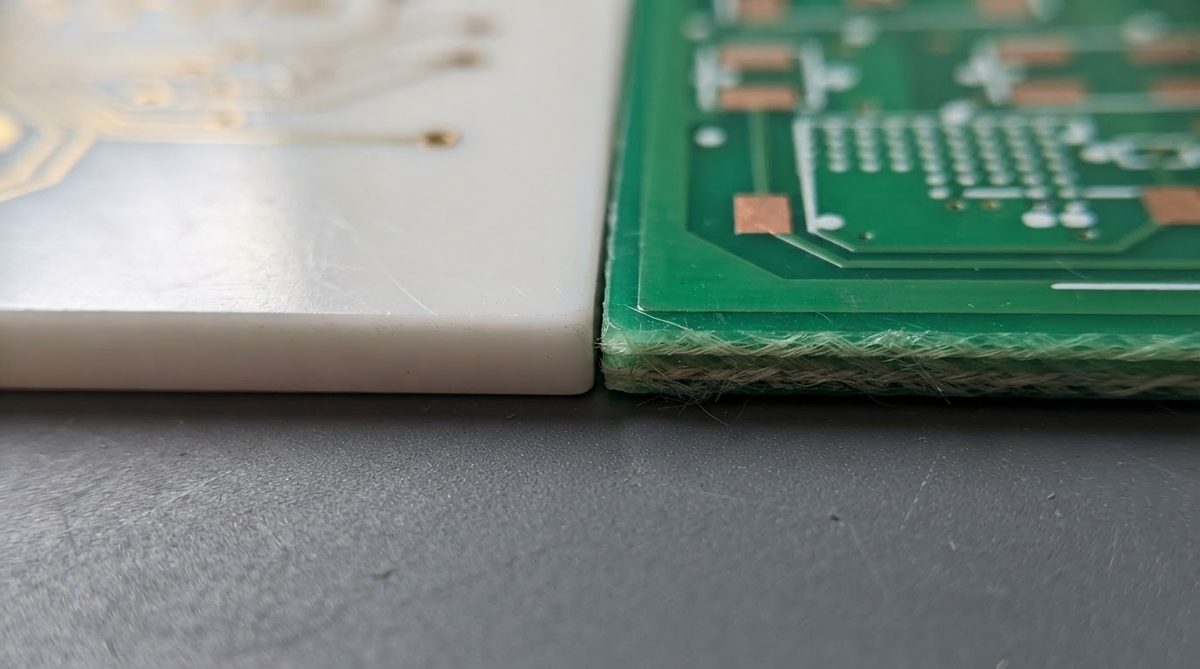
A vacuum outgassing PCB built on a ceramic substrate produces negligible volatile contamination because the fired inorganic body—Al₂O₃, AlN, or Si₃N₄—contains no polymer binder to release trapped gases. A 96% alumina substrate tested per ASTM E595 typically shows total mass loss (TML) below 0.01% and collected volatile condensable material (CVCM) below 0.001%, far under NASA’s screening limits of 1.0% TML and 0.1% CVCM. That makes ceramic the default substrate choice when contamination-sensitive optics, sensors, or spacecraft surfaces share the same vacuum volume as the circuit board.
Why Outgassing Matters for Vacuum PCB Applications
Any material placed inside a vacuum chamber or launched into orbit will release trapped gases and volatile organic compounds. Those volatiles condense on cooler surfaces—mirror coatings, detector windows, solar cells—degrading optical transmission and electrical performance. NASA’s ASTM E595 test (24 h at 125 °C, ≤5 × 10⁻⁵ torr) is the standard screening method. Components that exceed 1.0% TML or 0.1% CVCM are flagged for replacement or additional bake-out.
FR-4 (glass-epoxy) fails this screen easily: published TML values for standard FR-4 range from 0.5% to 1.8%, depending on resin system and moisture content, per NASA’s outgassing database. Polyimide flex (e.g., Kapton-based) performs better—TML around 0.9–1.2%—but still sits close to the limit and requires extended bake-out. A vacuum outgassing PCB built on ceramic sidesteps the problem entirely because there is no organic matrix to degas.
Vacuum Outgassing PCB Performance by Ceramic Substrate Type
| Material | TML (%) | CVCM (%) | Test Standard | Source |
|---|---|---|---|---|
| Al₂O₃ 96% | < 0.01 | < 0.001 | ASTM E595 | CoorsTek ADS-96R datasheet |
| Al₂O₃ 99.6% | < 0.01 | < 0.001 | ASTM E595 | Kyocera A-493 datasheet |
| AlN | < 0.01 | < 0.001 | ASTM E595 | Maruwa AN-230 datasheet |
| Si₃N₄ | < 0.01 | < 0.001 | ASTM E595 | Kyocera SN-220 datasheet |
| FR-4 (typical) | 0.5–1.8 | 0.02–0.15 | ASTM E595 | NASA GSFC outgassing database |
| Polyimide flex | 0.9–1.2 | 0.01–0.05 | ASTM E595 | NASA GSFC outgassing database |
Typical values for commercially available material, for comparison only. Confirm against the datasheet for your specific grade.
The ceramic substrate itself is not the whole story. Every material on the finished board contributes to total outgassing: solder paste flux residue, conformal coating, adhesives, and even surface finish chemistry. A vacuum outgassing PCB with a pristine ceramic substrate can still fail ASTM E595 if assembled with standard no-clean flux and not properly cleaned afterward.
Where the Outgassing Actually Comes From on a Ceramic PCB
Because the ceramic body contributes essentially zero volatiles, the outgassing budget of a finished ceramic assembly is dominated by these secondary sources:
- Solder flux residue. No-clean flux leaves organic residue that outgasses readily. Water-soluble or rosin-based fluxes, fully cleaned and verified with ionic contamination testing, are preferred for vacuum use.
- Solder alloy. Standard Sn-Ag-Cu (SAC305) is acceptable. Some high-temperature applications use Au-Sn (80/20), which has negligible outgassing and a reflow temperature of ~280 °C.
- Surface finish. ENIG and ENEPIG are common for space boards. Avoid OSP (organic solderability preservative)—it is an organic coating and adds measurable TML. See surface finish options for ceramic PCBs for a full comparison.
- Wire bond or die attach adhesive. Silver-filled epoxy adhesives vary widely; specify NASA-approved formulations (e.g., Ablebond 84-1LMISR4, TML 0.53%, CVCM 0.01%).
- Conformal coating. If required, use a qualified low-outgassing type such as Parylene C (TML ~0.1%, CVCM ~0.01%) rather than acrylic or silicone coatings.
Design Rules for Low-Outgassing Ceramic PCBs in Vacuum
Selecting a ceramic substrate is the first step. The rest of the design must follow vacuum-compatible practices. Here is a practical checklist:
- Specify cleaning level. Call out post-solder cleaning to MIL-STD-2000 or equivalent. Require ionic contamination below 1.56 µg NaCl/cm² (per IPC J-STD-001, Class 3).
- Eliminate blind cavities and trapped volumes. Any pocket that cannot be evacuated becomes a virtual leak. If your design requires blind vias, ensure they are either filled or vented through to the opposite side.
- Choose metallization carefully. Thick-film gold or DPC copper/gold are inorganic and add no outgassing. Avoid polymer thick-film conductors (silver-filled epoxy inks), which contain organic binders.
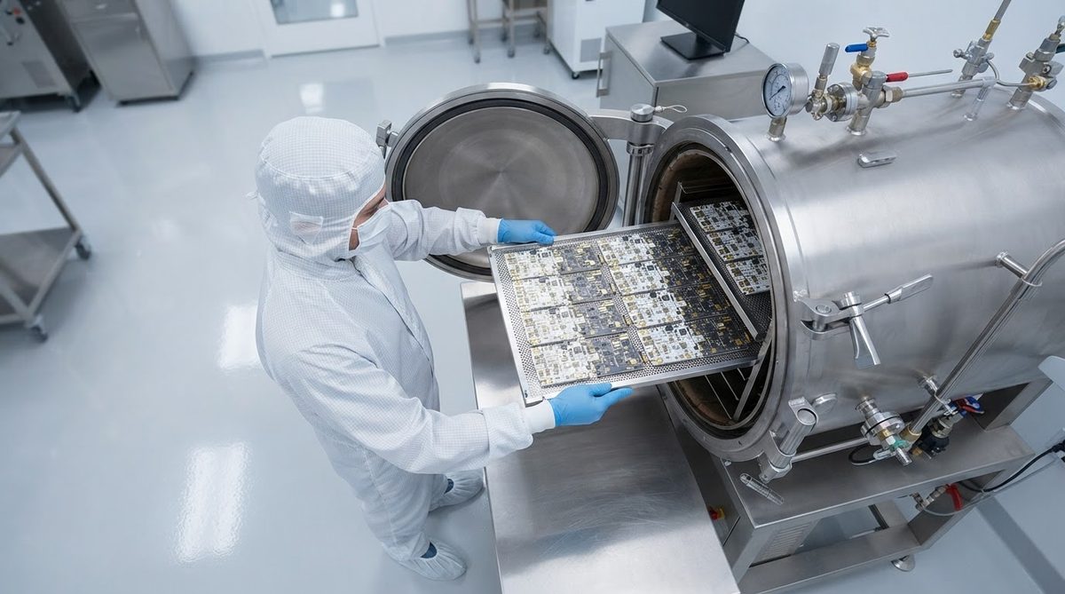
- Bake-out the finished assembly. Even a well-cleaned ceramic board benefits from a vacuum bake-out at 100–125 °C for 24–72 h before integration. This drives off adsorbed water and trace volatiles from secondary materials.
- Document everything. Space programs require full material disclosure. Maintain a materials list with ASTM E595 TML/CVCM data for every component, adhesive, and finish on the board.
Following ceramic PCB design guidelines from the start avoids late-stage redesigns that can introduce non-compliant materials.
Enter your substrate material, operating temperature, and environment below to see how thermal derating affects your vacuum outgassing PCB design margins.
Worked Example: Outgassing Budget for a Sensor Board
Consider a 25 × 25 mm Al₂O₃ 96% board carrying a MEMS sensor, assembled with SAC305 solder and ENIG finish, cleaned per IPC J-STD-001 Class 3, and baked out at 125 °C for 48 h.
Board mass: ~3.8 g (alumina density 3.7–3.9 g/cm³, 0.635 mm thick). At TML < 0.01%, the substrate contributes < 0.38 µg of mass loss. The dominant outgassing source is the die-attach adhesive—say 5 mg of silver epoxy at TML 0.53%, contributing ~26.5 µg. Total assembly TML is driven almost entirely by the adhesive, not the board. This illustrates why material selection for attach and encapsulation matters more than the substrate itself once you have chosen ceramic for your vacuum outgassing PCB.
Comparing Substrate Options for Vacuum Outgassing PCB Projects
| Parameter | Ceramic (Al₂O₃ 96%) | Polyimide Flex | FR-4 |
|---|---|---|---|
| TML (ASTM E595) | < 0.01% | 0.9–1.2% | 0.5–1.8% |
| CVCM (ASTM E595) | < 0.001% | 0.01–0.05% | 0.02–0.15% |
| Max continuous temp | 300–800 °C (material-dependent) | 200–260 °C | 130–140 °C |
| Thermal conductivity | 24–28 W/mK | 0.2–0.4 W/mK | 0.3–0.4 W/mK |
| CTE (ppm/°C) | 6.5–7.2 | 12–20 | 14–17 |
| Relative cost | 5–15× FR-4 | 2–5× FR-4 | 1× |
| Bake-out required? | Recommended (short) | Required (extended) | Often fails even after bake-out |
Typical values for commercially available material, for comparison only. Confirm against the datasheet for your specific grade.
When NOT to Use a Ceramic PCB for Vacuum
Ceramic is not always the right answer, even in vacuum. Consider alternatives when:
- The board is large and mechanically complex. Ceramic substrates are brittle and expensive above roughly 150 × 150 mm. A polyimide flex board with thorough bake-out may be more practical for large, low-power harnesses.
- Cost dominates and contamination tolerance is high. Industrial vacuum systems (coating chambers, leak detectors) often tolerate moderate outgassing. Standard FR-4 with a long bake-out may suffice if optics are not in the line of sight.
- High layer count is needed. Ceramic multilayer boards (HTCC or LTCC) can reach 10+ layers, but cost and lead time scale steeply. If your design needs 12 layers and fits within polyimide’s thermal envelope, a ceramic PCB cost analysis may not justify the switch.
- Mechanical shock is severe. Launch vibration is manageable with proper mounting, but ceramic boards are less forgiving of point impacts during handling than polymer boards. Factor in handling fixtures and conformal support.
Reliability in Thermal Vacuum Cycling
Space hardware faces repeated thermal vacuum (TVAC) cycles, often −55 °C to +125 °C. Ceramic substrates handle this range without degradation—alumina’s flexural strength (300–380 MPa per ASTM C1161) does not change meaningfully across this band. The weak point is the solder joint, especially where CTE mismatch exists between the ceramic (6.5–7.2 ppm/°C) and a component package (e.g., plastic QFP at 15–20 ppm/°C). Minimize large-footprint plastic packages, prefer leadless ceramic chip carriers or bare die, and qualify joints with thermal cycling per IPC-9701. For more on managing ceramic thermal management under TVAC conditions, review your thermal stack early in the design phase.
Frequently Asked Questions
Does a ceramic PCB need bake-out before vacuum use?
Yes, but the bake-out is short—typically 24 h at 100–125 °C. The ceramic itself holds negligible volatiles; the bake-out targets adsorbed water and trace residues from assembly materials. FR-4 and polyimide boards require 48–72 h or longer under the same conditions.
Can I use standard solder paste on a vacuum-grade ceramic board?
You can use standard SAC305 alloy, but you must fully clean the flux residue after reflow. No-clean flux is not acceptable for vacuum service because the residue outgasses organic compounds. Specify water-soluble flux with post-reflow aqueous cleaning and ionic contamination verification.
What surface finish is best for a space-rated ceramic PCB?
ENIG (electroless nickel / immersion gold) is the most common choice. It is inorganic, solderable, wire-bondable, and adds no measurable outgassing. ENEPIG adds a palladium barrier and is preferred when both gold wire bonding and soldering are needed on the same board. Avoid OSP, which is an organic finish.
Is LTCC suitable for vacuum and space applications?
Yes. LTCC (low-temperature co-fired ceramic) is used extensively in space-qualified RF modules and hermetic packages. The co-fired glass-ceramic body is fully sintered and contains no organics after firing. Outgassing is comparable to alumina substrates. Embedded conductors are typically silver or gold, both inorganic.
How do I get ASTM E595 data for a finished ceramic PCB assembly?
You test the complete assembly, not just the substrate. Submit a representative coupon—same materials, same process, same cleaning—to a lab accredited for ASTM E595 (e.g., NASA GSFC, Jet Propulsion Laboratory, or commercial labs like NTS or EAG Laboratories). Turnaround is typically 2–4 weeks. Many programs accept manufacturer-published data for individual materials combined into a worst-case outgassing budget, but flight qualification usually requires assembly-level testing.
Next Step
If you are specifying a vacuum outgassing PCB on ceramic for space or high-vacuum service, start with a DFM review to catch material and process choices that could compromise outgassing performance. Review ceramic PCB application examples for similar projects, then upload your files for a quote and flag the vacuum requirement so the engineering team can recommend the right substrate, metallization, and cleaning process for your contamination budget.