A ceramic PCB is made by forming a ceramic substrate from powder, applying conductive metal traces through metallization, and consolidating the assembly with heat. Understanding how ceramic PCB is made starts with recognizing that the exact sequence depends on the process family: co-fired (HTCC/LTCC), direct-plated copper (DPC), direct-bonded copper (DBC), or active metal brazing (AMB). Each route trades off resolution, thermal performance, and cost differently. Below is a step-by-step breakdown of how each one works.
Key Takeaways
- HTCC fires at 1 500–1 800 °C with tungsten or molybdenum conductors; LTCC fires at 850–900 °C and allows silver or gold.
- DPC produces the finest traces (line/space down to 20–50 µm) because it uses photolithography on a pre-fired substrate.
- DBC bonds a copper foil to Al₂O₃ or AlN at roughly 1 065 °C using a copper-oxide eutectic layer.
- AMB uses a titanium-bearing braze alloy at 800–900 °C and is the primary route for Si₃N₄ substrates in high-reliability power modules.
- All processes share two bookend steps: ceramic substrate preparation and post-metallization inspection.
Step 1 — How Ceramic PCB Is Made Begins with Substrate Preparation
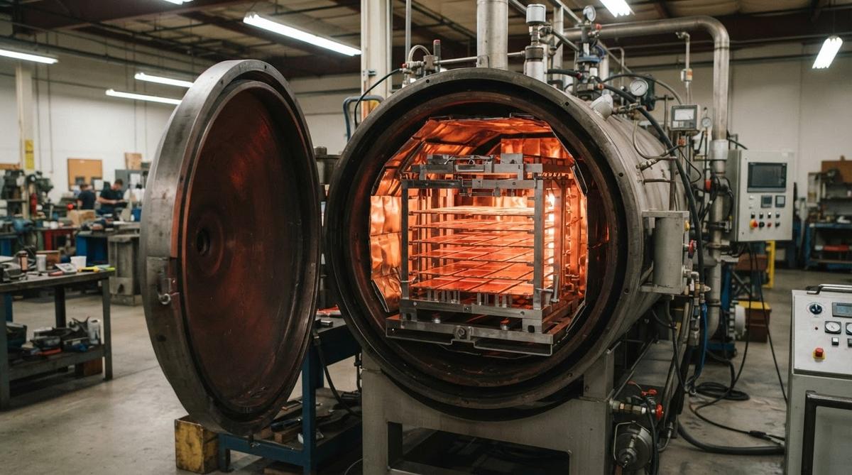
Every ceramic PCB starts as a powder. Alumina (Al₂O₃), aluminum nitride (AlN), or silicon nitride (Si₃N₄) powder is mixed with binders, plasticizers, and solvents to form a slurry. The slurry is cast into thin sheets called “green tape” using a doctor-blade process, or pressed into blanks by dry or isostatic pressing. Green tape thickness typically ranges from 0.1 mm to 1.0 mm per layer. You can read more about ceramic PCB substrate materials and their property differences in a separate guide.
For co-fired processes (HTCC and LTCC), the green tape remains unfired at this stage—metallization happens before sintering. For post-fire processes (DPC, DBC, AMB), the substrate is sintered first into a dense, finished ceramic blank, then metallized.
Step 2 — Via Formation
If the design requires interlayer connections, vias are punched or drilled into the green tape (co-fired) or laser-drilled into the sintered substrate (post-fire). Mechanical punching handles via diameters down to about 100 µm in green tape. Laser drilling on fired ceramic achieves diameters as small as 50 µm, depending on substrate thickness and material.
After drilling, vias are filled with conductive paste—tungsten or molybdenum for HTCC, silver or gold for LTCC, copper paste for DPC. The fill must be dense and flush; voids cause opens or thermal bottlenecks. Details on paste selection and fill quality are covered in the via filling for ceramic PCBs reference.
Step 3 — Metallization: The Five Main Routes
Metallization is where the process families diverge and where the question of how ceramic PCB is made gets its most varied answers. The choice determines conductor material, minimum feature size, thermal resistance, and cost.
HTCC (High-Temperature Co-Fired Ceramic)
Conductive paste—typically tungsten (W) or molybdenum (Mo)—is screen-printed onto each green-tape layer. Layers are stacked, aligned, and laminated under heat and pressure (roughly 70–80 °C, 20–30 MPa). The laminated stack is then co-fired in a reducing atmosphere (wet hydrogen) at 1 500–1 800 °C. Ceramic and metal sinter together into a monolithic body. Because the firing temperature is extreme, only refractory metals survive; copper, silver, and gold would melt or oxidize. HTCC conductors have higher resistivity than copper (W: ~5.5 µΩ·cm vs. Cu: ~1.7 µΩ·cm), which limits RF and high-current applications.
LTCC (Low-Temperature Co-Fired Ceramic)
LTCC uses a glass-ceramic composite tape that sinters at 850–900 °C. This lower temperature permits silver (Ag) or gold (Au) conductors, which have much lower resistivity than tungsten. The process sequence mirrors HTCC: print, stack, laminate, fire. LTCC excels in RF and microwave circuits because silver’s low loss tangent and the substrate’s tailorable dielectric constant (typically 5–9, depending on glass composition) enable precise impedance control. Layer counts of 10–40+ are common in LTCC modules.
DPC (Direct Plated Copper)
DPC starts with a pre-fired, polished ceramic substrate (usually Al₂O₃ 96 % or AlN). A thin adhesion layer (titanium, ~50 nm) and a copper seed layer (~200–300 nm) are deposited by sputtering or evaporation. Photoresist is applied, exposed, and developed to define the circuit pattern. Copper is then electroplated to the target thickness—commonly 1–3 oz (35–105 µm). After resist strip and seed-layer etch, the result is fine-line copper traces on a dense ceramic base. DPC achieves line/space of 20–50 µm, the finest of any ceramic PCB process. Learn more about metallization methods for ceramic PCBs in our dedicated comparison.
DBC (Direct Bonded Copper)
A copper foil (typically 0.1–0.6 mm thick) is placed on a pre-fired Al₂O₃ or AlN substrate. The assembly is heated to approximately 1 065 °C in a controlled atmosphere containing a small amount of oxygen. A thin copper-oxide eutectic layer forms at the interface, wetting the ceramic and bonding the foil. After cooling, the copper is patterned by photolithography and etching. DBC delivers thick copper for high-current paths but is limited in minimum trace width (typically ≥ 150 µm) because of the foil thickness. For designs that need heavy copper on ceramic substrates, DBC is the default choice.
AMB (Active Metal Brazing)
AMB bonds copper foil to ceramic using a braze alloy containing an active element—usually titanium (Ti). The braze (e.g., Ag-Cu-Ti) is applied as a paste or foil between the copper and substrate. The assembly is heated to 800–900 °C in vacuum (< 10⁻³ Pa). Titanium reacts with the ceramic surface to form a thin nitride or oxide reaction layer, creating a strong chemical bond. AMB is the primary method for Si₃N₄ substrates, which cannot be bonded by DBC because Si₃N₄ does not form a copper-oxide eutectic. AMB joints also exhibit higher peel strength (typically > 8 N/mm per IEC 62047) than DBC, making them preferred for power modules subject to thermal cycling.
Process Comparison Table
| Parameter | HTCC | LTCC | DPC | DBC | AMB |
|---|---|---|---|---|---|
| Firing / bonding temperature | 1 500–1 800 °C | 850–900 °C | N/A (room-temp plating) | ~1 065 °C | 800–900 °C |
| Conductor material | W, Mo | Ag, Au | Cu | Cu | Cu |
| Min line / space | 100–125 µm | 75–100 µm | 20–50 µm | 150–200 µm | 150–200 µm |
| Typical Cu thickness | N/A | N/A | 35–105 µm | 127–635 µm | 127–800 µm |
| Max layer count | 20+ | 40+ | 1–2 | 1–2 | 1–2 |
| Best suited for | Hermetic packages, sensors | RF modules, SiP | LED, fine-pitch IC | Power modules (IGBT) | Power modules (SiC, Si₃N₄) |
Typical values for commercially available processes, for comparison only. Confirm against the datasheet for your specific grade and supplier.
Step 4 — Sintering or Firing
For HTCC and LTCC, sintering is the critical consolidation step. The green body shrinks by 12–18 % linearly during firing as binders burn out and ceramic particles fuse. Shrinkage must be predicted and compensated in the artwork. Uneven shrinkage causes warping, delamination, or via misregistration. Furnace profiles are tightly controlled: a slow binder burnout ramp (1–3 °C/min through 300–500 °C), then a faster ramp to peak temperature, followed by a controlled cool-down.
DBC and AMB also involve a high-temperature step, but the substrate is already dense. The thermal profile controls the bonding reaction rather than ceramic densification. DPC skips high-temperature processing entirely after the initial substrate firing—its metallization occurs at or near room temperature.
Step 5 — Post-Processing and Surface Finish
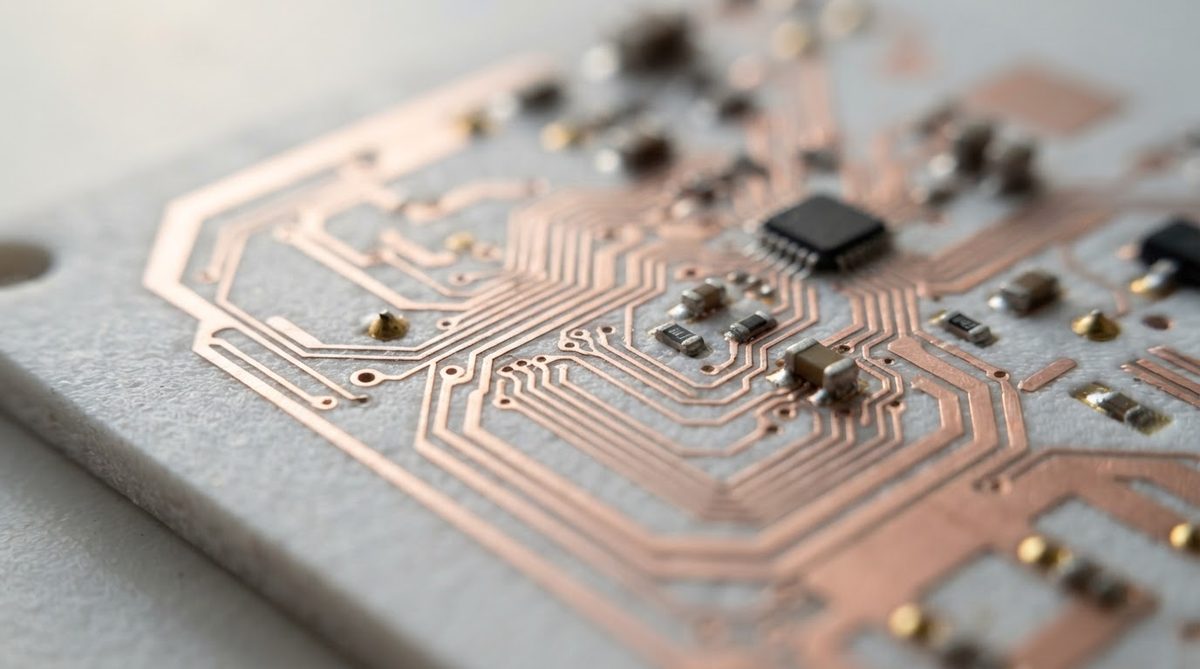
After metallization, several finishing steps follow:
- Patterning (DBC/AMB): Photoresist is applied to the bonded copper, exposed, developed, and the unwanted copper is etched away.
- Surface finish: Common options include ENIG (electroless nickel / immersion gold), ENEPIG, OSP, or direct gold plating. The choice depends on soldering method and wire-bondability requirements.
- Laser singulation or scribing: Panels are separated into individual units by laser cutting, diamond scribing, or CO₂ laser. Ceramic does not route like FR-4; mechanical routing causes cracking.
- Cleaning: Ultrasonic or plasma cleaning removes residues before final inspection.
Step 6 — Inspection and Quality Control
Ceramic PCBs undergo tighter inspection than organic boards because rework is limited and field failures in power or aerospace applications are costly. Typical checks include:
- AOI (automated optical inspection) for trace width, spacing, and pattern defects.
- X-ray inspection for via fill integrity and internal delamination in co-fired stacks.
- Hi-pot testing (dielectric withstand) per IPC-TM-650 or IEC 60243.
- Dimensional measurement against IPC-6012 or customer-specific tolerances.
- Thermal shock cycling (e.g., -55 °C to +150 °C, per MIL-STD-883) for reliability qualification.
For more on what temperatures ceramic substrates can survive in operation, see the guide on ceramic PCB maximum operating temperature.
Worked Example: HTCC 10-Layer Alumina Module
To illustrate how ceramic PCB is made in practice, consider a 10-layer HTCC module on 96 % Al₂O₃ with tungsten conductors, 50 mm × 50 mm finished size.
- Green tape casting: 10 sheets of 0.25 mm green tape (finished thickness ~0.21 mm after ~16 % linear shrinkage).
- Via punching: 150 µm diameter vias punched mechanically, filled with W paste.
- Screen printing: W paste printed on each layer; minimum line/space 125 µm.
- Lamination: Stacked and pressed at 75 °C, 25 MPa.
- Firing: Binder burnout at 400 °C for 4 hours, ramp to 1 600 °C, hold 2 hours, cool over 8 hours. Finished dimensions: ~42 mm × 42 mm (16 % shrinkage from 50 mm green size).
- Post-fire plating: Nickel + gold plated on exposed W pads for solderability.
- Singulation: Laser-scribed and snapped.
Total fired thickness: approximately 2.1 mm. The artwork was designed at 59.5 mm × 59.5 mm to compensate for shrinkage—this compensation factor is specific to the tape lot and must be verified with the supplier.
When NOT to Use a Ceramic PCB
Ceramic PCBs cost 5–20× more per unit area than FR-4 and 2–5× more than metal-core PCBs. If your board operates below 150 °C, dissipates under 1 W/cm², and does not require hermetic sealing or extreme dielectric strength, FR-4 or aluminum MCPCB will do the job at a fraction of the price. Ceramic is also brittle; boards larger than roughly 150 mm × 150 mm risk cracking during handling and assembly. For large-format, low-power designs, organic substrates are the practical choice.
FAQ
Can ceramic PCBs be made with standard FR-4 equipment?
No. Ceramic PCBs require specialized equipment: tape casting or powder pressing for substrates, high-temperature furnaces for sintering (up to 1 800 °C for HTCC), vacuum furnaces for AMB, and sputtering systems for DPC. Standard FR-4 lamination presses and drill spindles cannot process ceramic.
How long does it take to manufacture a ceramic PCB prototype?
Prototype lead times vary by process. DPC on a pre-fired substrate can be turned around in 5–10 working days. HTCC and LTCC prototypes typically take 2–4 weeks because of the multi-step co-firing cycle and shrinkage verification. DBC and AMB fall in between at 1–3 weeks.
Why does HTCC use tungsten instead of copper?
Copper melts at 1 085 °C. HTCC fires at 1 500–1 800 °C, well above copper’s melting point. Tungsten (melting point 3 422 °C) and molybdenum (2 623 °C) survive the firing cycle. The trade-off is higher electrical resistivity: tungsten’s bulk resistivity is roughly 3× that of copper.
What causes warping in co-fired ceramic boards?
Warping results from uneven shrinkage during sintering. Common causes include non-uniform tape thickness, inconsistent binder distribution, asymmetric conductor loading across layers, and improper furnace temperature uniformity. Designs with balanced metal density on top and bottom layers minimize warping.
Is it possible to make a double-sided ceramic PCB with DPC?
Yes. DPC can metallize both sides of a fired ceramic substrate. Through-vias are laser-drilled and filled with copper to connect the two sides. Double-sided DPC is common for LED submounts and small sensor boards where fine-pitch traces are needed on both faces.
Next Step
If you are evaluating how ceramic PCB is made for a specific design, start by reviewing ceramic PCB fabrication capabilities to match your requirements to a process. Ready to get pricing? Request a quote through the online form and include your Gerber files or a dimensioned sketch for the fastest turnaround.