This ceramic PCB FAQ collects the sixty questions hardware engineers, thermal designers, and sourcing managers ask most often — and answers each one with specific numbers, named standards, and honest trade-offs. Use the section headings to jump to the topic you need.
General — What Ceramic PCBs Are and Why They Exist
1. What is a ceramic PCB?
A ceramic PCB is a circuit board whose dielectric layer is a fired ceramic material — typically alumina (Al₂O₃), aluminum nitride (AlN), or silicon nitride (Si₃N₄) — instead of an organic resin like FR-4. The ceramic carries metallized traces (copper, silver, gold, or tungsten) applied by processes such as DPC, DBC, AMB, thick film, HTCC, or LTCC. For a full definition, see what a ceramic PCB is.
2. Why use a ceramic PCB instead of FR-4?
Ceramic substrates offer higher thermal conductivity (24–200 W/mK vs. 0.3 W/mK for FR-4), near-zero moisture absorption (< 0.02%), stable dielectric constant up to GHz frequencies, and continuous operating temperatures above 300 °C. They make sense when heat, frequency, or environment rules out organics. More detail is in our guide to why engineers choose ceramic PCBs.
3. What are the main disadvantages?
Cost (3–10× higher than FR-4 per unit area), brittleness (flexural strength of 96 % alumina is ~340 MPa per ASTM C1161, but zero plastic deformation before fracture), limited panel size (typically ≤ 190 mm × 140 mm for DPC), and longer lead times. Read the full breakdown of ceramic PCB advantages and disadvantages.
4. When is a ceramic PCB actually worth the cost?
When any of these are true: junction temperature must stay below a critical threshold that FR-4 or MCPCB cannot meet; the board operates above 250 °C continuously; the application demands hermeticity or near-zero outgassing (space, vacuum, medical implant); or the RF loss tangent of organics is too high above 5 GHz. If none apply, FR-4 or metal-core is usually the better call. See when a ceramic PCB is actually worth it.
5. What is DPC ceramic technology?
DPC (Direct Plated Copper) deposits a thin sputtered seed layer on a fired ceramic substrate, then builds copper traces by photolithography and electroplating. It achieves fine line/space (down to 30 µm in production) and smooth surfaces suitable for die attach. Learn more about DPC ceramic technology.
6. What is the difference between DBC and AMB?
DBC (Direct Bonded Copper) bonds a copper foil to ceramic at ~1065 °C using a Cu–O eutectic. AMB (Active Metal Brazing) uses a Ti-containing braze alloy at ~850 °C. AMB produces a stronger bond on AlN and Si₃N₄ and survives more thermal cycles, but costs more. DBC is common on Al₂O₃; AMB dominates on AlN and Si₃N₄ power modules.
7. What is the difference between HTCC and LTCC?
HTCC (High-Temperature Co-fired Ceramic) fires above 1 500 °C with tungsten or molybdenum conductors. LTCC fires at 850–900 °C and allows silver or gold conductors with lower resistivity. LTCC enables embedded passives and multilayer structures more easily. Neither process uses AlN or Si₃N₄ substrates.
8. Can a ceramic PCB be multilayer?
Yes. LTCC routinely produces 10–40+ layers. HTCC supports similar counts. DPC and DBC are typically single- or double-sided, though stacked assemblies with bonding layers are possible.
Materials — Choosing the Right Ceramic
9. What ceramic materials are used for PCBs?
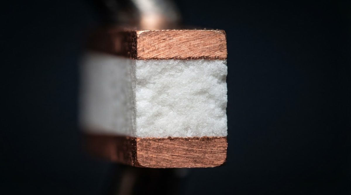
The most common are 96 % alumina (Al₂O₃), 99.6 % alumina, aluminum nitride (AlN), and silicon nitride (Si₃N₄). Specialty substrates include zirconia-toughened alumina (ZTA), beryllium oxide (BeO — a regulated carcinogen; see safety note below), and various glass-ceramic LTCC tapes.
10. What is the thermal conductivity of each material?
| Material | Thermal conductivity | Unit | Condition | Source |
|---|---|---|---|---|
| Al₂O₃ 96 % | 24–28 | W/mK | 20 °C | CoorsTek ADS-996 datasheet |
| Al₂O₃ 99.6 % | 28–35 | W/mK | 20 °C | Kyocera A-493 datasheet |
| AlN | 170–200 | W/mK | 20 °C | Maruwa AN-200 datasheet |
| Si₃N₄ | 70–90 | W/mK | 20 °C | Kyocera SN-90 datasheet |
| BeO 99.5 % | 250–300 | W/mK | 20 °C | Materion Thermalox 995 datasheet |
| LTCC (typical) | 2–4 | W/mK | 20 °C | DuPont 951 Green Tape datasheet |
Typical values for commercially available material, for comparison only. Confirm against the datasheet for your specific grade.
11. Is BeO safe to use?
Beryllium oxide dust is a confirmed human carcinogen and causes chronic beryllium disease (CBD). Intact sintered BeO substrates can be handled with standard PPE, but any machining, grinding, or breakage that generates dust requires full engineering controls per OSHA 29 CFR 1910.1024. Most new designs avoid BeO unless no alternative meets the thermal budget.
12. Which ceramic has the best CTE match to silicon?
AlN at 4.5 ppm/°C (20–400 °C) is closest to silicon’s 2.6–3.5 ppm/°C. Al₂O₃ at 7.1 ppm/°C and Si₃N₄ at 2.7 ppm/°C are the next options. Si₃N₄ matches silicon even more closely, but its lower thermal conductivity (70–90 W/mK) limits its use in high-flux applications.
13. Which ceramic is strongest?
Si₃N₄ has the highest flexural strength among common PCB ceramics: 600–900 MPa (ASTM C1161, 3-point bend). Compare that with 340 MPa for 96 % alumina and 300–350 MPa for AlN. Si₃N₄ is the go-to substrate for power modules that undergo severe thermal cycling (e.g., EV traction inverters).
14. Does ceramic absorb moisture?
Virtually none. Sintered 96 % alumina has water absorption < 0.02 % per ASTM C373. This means ceramic PCBs do not need baking before reflow, unlike some organic boards. More on this at ceramic PCB moisture absorption.
Dimensions, Thickness, and Weight
15. How thin can a ceramic PCB be?
Commercially available alumina substrates go down to 0.1 mm (100 µm). AlN substrates are commonly available at 0.25 mm minimum. Thinner is possible with custom lapping, but handling fragility rises sharply. Details at how thin a ceramic PCB can be.
16. What standard thicknesses are available?
Common stock thicknesses for Al₂O₃: 0.25, 0.38, 0.50, 0.635, 1.0, and 2.0 mm. AlN is typically stocked in 0.25, 0.50, 0.635, and 1.0 mm.
17. What is the maximum substrate size?
This varies by process and manufacturer. DPC panels are often limited to around 140 × 190 mm. DBC can run larger blanks (up to ~190 × 280 mm). LTCC panels can reach 200 × 200 mm before co-firing shrinkage.
18. Are ceramic PCBs heavier than FR-4?
Yes. Al₂O₃ has a density of ~3.7–3.9 g/cm³ vs. ~1.85 g/cm³ for FR-4. A 1 mm thick, 25 × 25 mm alumina substrate weighs roughly 2.4 g compared to ~1.2 g for the same FR-4 piece. For weight-critical designs, see ceramic PCB weight vs. FR-4.
19. Can ceramic substrates be cut or scored after metallization?
Yes. Laser scribing, diamond sawing, and water-jet cutting are all used. Laser scribing is the most common method for creating snap lines on thin alumina.
Thermal Performance
20. What is the maximum operating temperature of a ceramic PCB?
The ceramic itself survives well above 1 000 °C. The practical limit is set by the metallization and solder: thick-film gold/silver conductors are stable to ~500 °C; DBC copper to ~400 °C in inert atmosphere; standard SAC305 solder to ~220 °C peak. System-level max operating temperature is typically 300–350 °C for specialized assemblies.
21. How do I calculate thermal resistance through a ceramic substrate?
Use Rth = t / (k × A), where t = substrate thickness, k = thermal conductivity, A = heat-spreading area. Example: a 0.635 mm thick, 10 × 10 mm AlN substrate (k = 180 W/mK) gives Rth = 0.000635 / (180 × 0.0001) = 0.035 °C/W. The same geometry in 96 % alumina (k = 25 W/mK) gives 0.254 °C/W — about 7× higher.
22. Does thermal conductivity change with temperature?
Yes. AlN’s thermal conductivity drops from ~180 W/mK at 25 °C to ~100 W/mK at 300 °C (Maruwa datasheet). Alumina is more stable: ~25 W/mK at 25 °C, ~15 W/mK at 300 °C. Always derate for your actual operating temperature.
23. Can ceramic PCBs replace heat sinks?
In low-power applications (under ~2 W), a ceramic substrate with adequate copper area can serve as the primary thermal path to ambient, eliminating a separate heat sink. Above that, the substrate conducts heat to a heat sink or chassis — it does not replace it.
Soldering and Assembly
24. Can you solder to a ceramic PCB?
Yes. Standard SMT reflow (SAC305, peak 245 °C) works on metallized ceramic substrates just as on FR-4. The key difference is that ceramic has no glass transition temperature, so the substrate is thermally stable through reflow. Detailed guidance at soldering to a ceramic PCB.
25. What solder paste should I use?
For most applications, SAC305 (Sn96.5/Ag3.0/Cu0.5) with a no-clean flux works well. For high-temperature service above 200 °C, consider high-lead (Pb93.5/Sn5/Ag1.5, liquidus 296 °C) or AuSn (Au80/Sn20, liquidus 280 °C) solder.
26. Do I need a special reflow profile?
Ceramic has very low thermal mass per unit area compared to thick FR-4 assemblies, so it heats and cools faster. Use a slower ramp rate (1–2 °C/s) to avoid thermal shock to components. Peak temperature and time above liquidus follow normal IPC J-STD-020 guidelines.
27. Can I hand-solder to ceramic?
Yes, provided the pad metallization is solderable (ENIG, ENEPIG, or tin-plated copper). Use a temperature-controlled iron at 350–370 °C and avoid pressing the tip hard against the substrate — ceramic is brittle and a point load can crack thin substrates.
28. Can I wire-bond to a ceramic PCB?
Yes. Gold wire bonding works on thick-film gold pads or ENIG-finished DPC copper pads. Aluminum wedge bonding works on bare copper or nickel-plated pads. Surface roughness must be controlled: Ra < 0.4 µm is typical for reliable Au ball bonds.
Electrical Properties
29. What is the dielectric constant of alumina?
96 % alumina has a dielectric constant (εr) of 9.0–9.5 at 1 MHz (per CoorsTek ADS-996). This is significantly higher than FR-4 (εr ~4.3), which affects impedance calculations. AlN is ~8.5–9.0; Si₃N₄ is ~7.5–8.0.
30. What is the dielectric breakdown voltage?
96 % alumina: 10–15 kV/mm (per ASTM D149). AlN: 15–17 kV/mm. These values are far above FR-4 (~20 kV/mm for 1.6 mm thickness, but only ~1 kV/mm at thin sections). Ceramic excels in high-voltage isolation.
31. Is ceramic good for RF and microwave?
Alumina’s loss tangent (tan δ) is 0.0001–0.0003 at 10 GHz, roughly 100× lower than FR-4 (~0.02). This makes it excellent for filters, couplers, and antenna feeds above 1 GHz. LTCC adds the benefit of embedded passives and multilayer stripline.
32. Can I run controlled impedance on ceramic?
Yes, but the high εr means traces are narrower for a given impedance. A 50 Ω microstrip on 0.635 mm alumina (εr = 9.4) requires a trace width of roughly 0.6 mm — about half the width needed on FR-4 at the same thickness. Use a field solver, not rule-of-thumb calculators calibrated for organics.
Reliability and Lifespan
33. How long does a ceramic PCB last?
The ceramic substrate itself does not degrade chemically or thermally under normal conditions. Failure modes are mechanical (cracking from shock or thermal cycling) and metallurgical (solder fatigue, copper delamination). Well-designed DBC assemblies on alumina pass 3 000+ thermal cycles from –40 to +150 °C per IEC 60749-34.
34. What causes ceramic PCBs to fail?
The three most common failure modes are: (1) substrate cracking from mechanical shock or improper mounting, (2) copper trace delamination after extended thermal cycling, and (3) solder joint fatigue from CTE mismatch between component and substrate.
35. Is a ceramic PCB brittle?
Yes. Ceramic has zero ductility — it fractures without warning. Handle substrates on edges, use vacuum wands for placement, and never clamp directly on the ceramic surface. See our handling guide on ceramic PCB brittleness and crack risk.
36. Can ceramic PCBs survive thermal shock?
AlN and Si₃N₄ tolerate rapid temperature changes better than alumina due to higher thermal conductivity and (for Si₃N₄) higher fracture toughness. 96 % alumina can survive a ΔT of ~200 °C in a single quench (per Hasselman thermal shock resistance parameter), while Si₃N₄ handles ΔT > 600 °C.
Cost and Ordering
37. How much does a ceramic PCB cost?
Rough ranges for a single-sided DPC alumina board, 25 × 25 mm, in quantities of 100: $3–$8 per piece. AlN substrates run 3–5× more. Prices drop significantly at 1 000+ pieces. LTCC multilayer boards are quoted per design due to tooling.
38. What drives ceramic PCB cost?
Material grade (AlN >> Al₂O₃), substrate area, copper thickness, number of layers, minimum feature size, surface finish, and quantity. Tooling for laser or screen printing is a fixed cost that amortizes over volume.
39. Can I order a single piece?
Many manufacturers accept single-piece prototype orders, though the per-unit cost is high because setup and inspection time is fixed.
40. What is a typical prototype lead time?
5–15 working days for DPC on alumina, depending on complexity. LTCC prototypes take 3–5 weeks due to tape preparation and co-firing.
Design Rules
41. What is the minimum trace and space for DPC?
Production-proven minimums are 30/30 µm (line/space) for DPC on polished alumina. Thick film is coarser: 100–150 µm line/space. DBC is coarser still: 200–300 µm.
42. Can I put vias in a ceramic PCB?
Yes. Laser-drilled or punched vias filled with tungsten (HTCC), silver (LTCC), or plated copper (DPC) are standard. Via diameters range from 50 µm (laser) to 200+ µm (mechanical punch). For double-sided DPC, see connecting top and bottom on a double-sided substrate.
43. What surface finishes are available?
Common options: ENIG, ENEPIG, bare copper (with OSP), immersion silver, electrolytic gold, and thick-film gold. The choice depends on wire-bonding requirements, solderability, and shelf life.
44. Should I panelize ceramic PCBs?
Yes, if your design allows it. Laser-scribed break lines let you snap individual boards from a panel after assembly, reducing handling costs. Leave ≥ 0.5 mm between scribe lines and the nearest pad.
45. What file formats do I need for quoting?
Gerber RS-274X or Gerber X2 for copper layers, drill files in Excellon format, and a fabrication drawing (PDF) showing dimensions, tolerances, material callout, and finish. An ODB++ package is also accepted by most fabs.
Handling, Storage, and ESD
46. How should I store ceramic PCBs?
In a dry, dust-free environment at 15–30 °C and < 60 % RH. Ceramic does not absorb moisture, so baking before use is not required. Keep substrates in waffle trays or interleaved with lint-free paper to prevent edge chipping.
47. Do ceramic PCBs need ESD precautions?
The substrate itself is an insulator with high surface resistivity (> 10¹⁴ Ω). Static charge can build up and damage sensitive components during assembly. Standard ESD practices (wrist straps, ionizers, conductive work surfaces) apply.
48. What is the shelf life of a metallized ceramic PCB?
With ENIG or electrolytic gold finish, shelf life exceeds 12 months in proper storage. Bare copper finishes oxidize and should be soldered within 2–4 weeks, or protected with OSP.
Applications
49. Where are ceramic PCBs used?
Power electronics (IGBT modules, SiC/GaN driver stages), LED lighting (high-flux COB arrays), RF/microwave (filters, amplifiers, radar), medical devices (implants, imaging sensors), automotive (ADAS lidar, EV inverters), aerospace (satellite transponders), and sensors (MEMS, gas sensors, thermocouples).
50. Are ceramic PCBs used in space?
Yes. Ceramic substrates meet NASA outgassing requirements (ASTM E595: TML < 1.0 %, CVCM < 0.1 %) inherently because they contain no organic volatiles. HTCC and LTCC hermetic packages are standard in satellite electronics.
51. Are ceramic PCBs used in medical implants?
Yes. Alumina is biocompatible (ISO 10993 tested) and used in cochlear implants, neural stimulators, and pacemaker hybrid circuits. Hermeticity prevents body fluid ingress.
Comparison with Alternatives
52. Ceramic PCB vs. metal-core PCB (MCPCB)?
MCPCB uses an aluminum or copper base with a thin dielectric layer (1–8 W/mK). It is cheaper and easier to machine but has lower dielectric strength and cannot operate above ~150 °C continuously. Ceramic wins on isolation voltage, operating temperature, and RF performance. MCPCB wins on cost and mechanical robustness.
53. Ceramic PCB vs. IMS (Insulated Metal Substrate)?
IMS is essentially the same as MCPCB. The dielectric layer thermal conductivity (typically 1–3 W/mK) is the bottleneck. Ceramic removes that bottleneck because the entire substrate is the dielectric and the thermal conductor simultaneously.
54. Ceramic PCB vs. Rogers/PTFE?
Rogers laminates (e.g., RO4003C, RT/durosid 5880) offer low loss tangent for RF, but their thermal conductivity is only 0.6–0.8 W/mK. Ceramic is preferred when both RF performance and thermal management matter — for example, GaN power amplifiers above 6 GHz.
55. Ceramic PCB vs. polyimide flex?
Polyimide flex offers mechanical flexibility that ceramic cannot provide. Choose ceramic when the board is rigid-mounted and thermal or high-frequency performance is the priority. Choose flex when the board must bend or fold.
Environmental and End-of-Life
56. Are ceramic PCBs RoHS compliant?
The ceramic substrate itself contains no restricted substances under RoHS (Directive 2011/65/EU). Compliance depends on the solder, finish, and components used. Lead-free finishes (ENIG, immersion silver) and SAC305 solder keep the full assembly compliant.
57. Can ceramic PCBs be recycled?
Copper can be recovered from metallized ceramic by chemical stripping or smelting. The ceramic substrate is inert and can be crushed for use as an abrasive or filler. Precious metals (gold, silver) are economically recoverable.
58. Are ceramic PCBs classified as hazardous waste?
Standard alumina, AlN, and Si₃N₄ substrates are not hazardous. BeO substrates are regulated as hazardous due to beryllium content and require special disposal per local regulations.
Machining and Post-Processing
59. How do I drill holes in a ceramic substrate?
Laser drilling (CO₂ or UV) is the most common method for holes under 300 µm. Mechanical drilling with diamond-coated bits works for larger holes but risks edge chipping. Ultrasonic machining is used for complex shapes.
60. How do I cut ceramic substrates to size?
Laser scribing and snapping is the standard production method. Diamond dicing saws give clean edges for precision work. Water-jet cutting handles thick substrates without thermal stress.
When Not to Use a Ceramic PCB
Ceramic is the wrong choice when:
- Your thermal load is under 1 W/cm² and a standard FR-4 board with thermal vias handles it.
- The board is larger than ~150 × 200 mm — organic or metal-core substrates are more practical at that scale.
- The product is cost-sensitive consumer electronics where the board cost matters more than long-term reliability.
- The board must flex, fold, or absorb mechanical impact — use polyimide flex or rigid-flex instead.
- You need more than 6–8 layers with fine-pitch BGAs — standard HDI on organic laminates is more mature and cheaper.
Next Step
If your project fits the profile above, start with a material selection: 96 % alumina for most thermal and RF work, AlN when you need 170+ W/mK conductivity or tight CTE match to silicon, Si₃N₄ for extreme thermal cycling. Upload your Gerbers for a quote at AluminaPCB’s instant quote page and an engineer will review your design files within one business day.