Electroplating vs electroless copper is the central metallization decision on any ceramic PCB. Electroplated copper uses external current to deposit copper at 15–25 µm/hour, producing thick, dense traces with bulk-like conductivity. Electroless copper is an autocatalytic chemical process that deposits copper at roughly 1–5 µm/hour without current, yielding thin, uniform layers even on non-conductive ceramic surfaces. Most ceramic PCB metallization schemes use both: electroless copper first as a seed layer, then electroplating to build the conductor to final thickness.
Key Takeaways
- Electroless copper deposits at 1–5 µm/hour and is limited to roughly 0.5–5 µm per pass; electroplating deposits at 15–25 µm/hour and can reach 35–300 µm.
- Electroless copper coats non-conductive alumina and AlN directly; electroplating requires a conductive seed layer first.
- Electroplated copper achieves ≥95% IACS conductivity; electroless copper typically reaches 70–85% IACS due to incorporated phosphorus or formaldehyde byproducts.
- For high-current power circuits on ceramic, electroplating is the practical choice for the bulk conductor. Electroless is the enabler that makes it possible.
How Electroplating vs Electroless Copper Works on Ceramic Substrates
Electroless Copper Deposition
The ceramic substrate is cleaned, activated with a palladium-tin catalyst, and immersed in a bath containing copper sulfate and a reducing agent (typically formaldehyde or glyoxylic acid). Copper ions reduce onto the catalyzed surface without any external power supply. The deposit grows at a self-limiting rate, and bath chemistry must be tightly controlled to avoid spontaneous decomposition. On alumina or AlN, this step is essential because the ceramic is electrically insulating and cannot serve as a cathode for direct electroplating.
Electroless baths deposit copper with 2–8 wt% phosphorus incorporation (depending on formulation), which raises resistivity. The resulting film is adequate as a seed layer or a thin functional conductor for low-current RF traces, but it is not a substitute for electroplated copper where bulk conductivity matters. Adhesion to ceramic depends heavily on surface preparation: mechanical roughening, plasma treatment, or a sputtered Ti/TiW adhesion layer all improve peel strength significantly.
Electroplating
Once a conductive seed exists, the substrate is immersed in an acid copper sulfate bath and connected as the cathode. An external DC or pulse-reverse current drives copper deposition. The plating rate, grain structure, and throwing power are controlled by current density, bath additives (brighteners, levelers, suppressors), and agitation. Electroplated copper on ceramic PCBs typically targets 18–70 µm for signal and power traces, though DBC and AMB processes bond copper foils of 127–300 µm that are then patterned rather than plated.
The main advantage of electroplating is speed and purity. A 35 µm copper layer takes roughly 1.5–2 hours to plate, versus days of electroless deposition for the same thickness (which is impractical). Conductivity of electroplated copper is 5.7–5.8 × 10⁷ S/m at 20 °C, essentially matching bulk copper per ASTM B193.
Electroplating vs Electroless Copper: Property Comparison
| Parameter | Electroless Cu | Electroplated Cu | Unit | Condition / Source |
|---|---|---|---|---|
| Deposition rate | 1–5 | 15–25 | µm/hr | Typical acid baths; varies by chemistry |
| Practical thickness range | 0.3–5 | 5–300 | µm | Single-pass (electroless) vs. timed plate |
| Electrical conductivity | 70–85 | ≥95 | % IACS | 20 °C; ASTM B193 |
| Resistivity | 2.0–2.5 | 1.7–1.8 | µΩ·cm | 20 °C |
| Phosphorus content | 2–8 | <0.01 | wt% | Depends on bath reducer |
| Uniformity on complex geometry | Excellent (±5%) | Fair (±10–20%) | — | Through-holes and blind vias |
| Requires conductive seed? | No | Yes | — | — |
| Tensile strength (as-deposited) | 350–550 | 200–350 | MPa | Electroless higher due to P; per MIL-C-26074 |
| Ductility (elongation) | 3–8 | 12–25 | % | As-deposited; annealing improves both |
Typical values for commercially available chemistries, for comparison only. Confirm against your plating supplier’s process data.
The table above summarizes the core trade-off in electroplating vs electroless copper: electroless excels at uniform, thin coatings on insulating surfaces, while electroplating delivers the thickness and conductivity needed for power and signal traces.
Why Ceramic PCBs Typically Use Both Methods
A common DPC (direct plated copper) process flow on an Al₂O₃ 96% substrate illustrates why electroplating vs electroless copper is not an either/or decision — the two methods are complementary:
- Sputter Ti/Cu seed — a 50–200 nm titanium adhesion layer followed by 200–500 nm copper, deposited by magnetron sputtering.
- Electroless Cu build-up — optional step to thicken the seed to ~1–2 µm for better current distribution during plating.
- Photoresist pattern — dry film laminated and exposed to define traces.
- Electroplate Cu — acid copper sulfate bath, 2–4 A/dm², 35–70 µm target thickness.
- Strip, etch seed — resist stripped, exposed seed etched to isolate traces.
In this flow, electroless copper is the bridge between the non-conductive ceramic and the high-rate electroplating step. Skipping it is possible if the sputtered seed is thick and uniform enough, but many fabricators include a flash electroless layer to reduce pinhole density and improve plating uniformity in via structures.
Worked Example: Trace Resistance Comparison
Suppose you need a 10 mm long, 0.5 mm wide power trace carrying 2 A on an alumina substrate. Compare a 5 µm electroless-only conductor to a 35 µm electroplated conductor — a practical illustration of the electroplating vs electroless copper performance gap.
Electroless Cu (ρ ≈ 2.2 µΩ·cm):
R = ρ × L / (W × t) = 2.2 × 10⁻⁶ Ω·cm × 1.0 cm / (0.05 cm × 0.0005 cm) = 88 mΩ
Power loss at 2 A: P = I²R = 4 × 0.088 = 352 mW
Electroplated Cu (ρ ≈ 1.72 µΩ·cm):
R = 1.72 × 10⁻⁶ × 1.0 / (0.05 × 0.0035) = 9.8 mΩ
Power loss at 2 A: P = 4 × 0.0098 = 39 mW
The electroplated trace dissipates roughly 9× less power. For a sensor signal line carrying microamps, the electroless layer alone might suffice. For anything above a few hundred milliamps, the resistance penalty of thin electroless copper becomes significant.
Adhesion to Ceramic: The Critical Difference
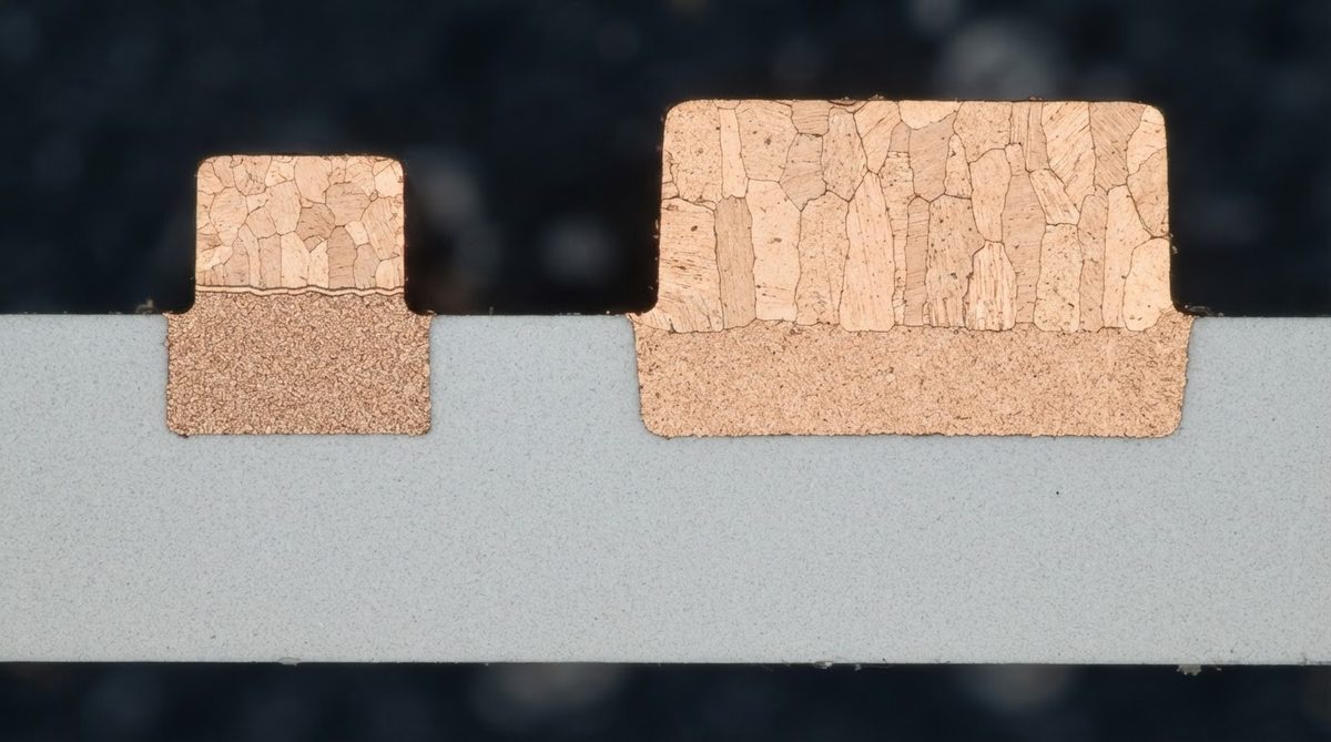
Neither electroless nor electroplated copper bonds strongly to bare, smooth ceramic on its own. Peel strength depends almost entirely on the adhesion layer beneath the copper. On DPC substrates, a sputtered titanium or titanium-tungsten layer provides chemical bonding to the oxide surface. On thick-film hybrid circuits, a printed and fired copper or silver-palladium paste anchors into the ceramic’s surface porosity.
Electroless copper deposited directly on activated ceramic (without a sputtered adhesion layer) typically achieves peel strengths of 2–4 N/cm. With a Ti/Cu sputter seed underneath, peel strength rises to 8–15 N/cm, comparable to DBC bonding. If your application demands high peel strength, the choice between silver and copper metallization matters as much as the deposition method.
When NOT to Use Electroplated Copper
Electroplating is the wrong choice in several situations:
- Extremely thin, uniform coatings (<1 µm). Electroless deposition is more uniform at sub-micron thicknesses. Electroplating at very low current densities is slow and prone to nodules.
- Non-conductive substrates with no seed layer budget. If your process cannot include sputtering or evaporation, electroless is the only chemical route to metallize bare ceramic.
- Through-via fill on high-aspect-ratio holes. Electroless copper’s superior throwing power coats the inside of deep vias more uniformly than electroplating, which tends to plate faster at the via mouth (“dog-boning”).
- Cost-sensitive prototypes with thin conductors. A single electroless step avoids the capital and chemistry management of a plating line. For prototype versus production runs, the simpler process can shorten turnaround.
Conversely, if you need copper thicker than about 5 µm, or your circuit carries meaningful current, electroplating is the practical path. Electroless-only builds above 5 µm are slow, expensive, and produce higher-resistivity conductors.
When NOT to Use Electroless Copper Alone
Relying solely on electroless copper fails when:
- Trace resistance matters — the 70–85% IACS conductivity and thin deposit create unacceptable I²R losses in power circuits.
- Wire bonding or heavy soldering loads demand thick, ductile copper. Electroless films are harder but more brittle.
- High-frequency RF designs need low-loss conductors. The higher resistivity of electroless copper increases skin-effect losses above 1 GHz. For RF substrates, consider how ceramic compares to FR-4 in dielectric loss as well.
FAQ
Can you electroplate directly onto bare alumina ceramic?
No. Alumina is an electrical insulator, so it cannot act as a cathode. You must first deposit a conductive seed layer by sputtering, evaporation, or electroless plating before electroplating copper onto ceramic.
Does electroless copper corrode faster than electroplated copper?
Electroless copper with high phosphorus content (6–8 wt%) actually resists corrosion better than pure electroplated copper because the phosphorus forms a passive barrier layer. Low-phosphorus electroless deposits behave more like pure copper in corrosive environments.
What thickness of electroless copper is needed as a seed for electroplating?
A minimum of 0.3–0.5 µm of electroless copper is standard for reliable electroplating. Thinner seeds risk incomplete coverage and plating voids. Many fabricators target 1–2 µm to ensure low sheet resistance and uniform current distribution during the subsequent plating step.
Is electroless copper plating more expensive per micron than electroplating?
Yes. Electroless baths use expensive reducing agents and palladium catalysts, and deposit copper 5–15× slower. For films above 5 µm, electroplating is significantly cheaper per micron of deposited copper. Electroless is cost-effective only for thin seed layers or specialized conformal coatings.
Can I use electroless nickel instead of electroless copper on ceramic?
Electroless nickel (EN) is common for barrier and solderable layers, but its resistivity (60–90 µΩ·cm) is 30–50× higher than copper. EN is not a substitute for copper as a signal or power conductor. It is typically deposited over copper as a diffusion barrier before a gold or ENIG finish, as discussed in context with substrate material selection for power modules.
Next Step
If you are specifying copper metallization on a ceramic substrate, the deposition method should match your thickness requirement, current load, and process budget. For most power and RF applications, a sputtered seed plus electroplated copper is the standard approach. Share your stackup and copper thickness target with our engineering team to get a process recommendation and quote.