A well-designed ceramic PCB routinely lasts 25 years or more in continuous service, far exceeding the 10–15 year practical life of FR-4 in comparable thermal and chemical environments. The substrate itself does not degrade the way organic laminates do: alumina and aluminum nitride are chemically inert, dimensionally stable, and immune to moisture absorption. What actually limits ceramic PCB lifespan is almost always a failure at an interface—solder joints, metallization adhesion, or mechanical mounting—not the ceramic body.
Key Takeaways
- Ceramic substrates (Al₂O₃, AlN, Si₃N₄) show no measurable property degradation after 100,000+ hours at 300 °C in air.
- Thermal-cycle fatigue of solder joints and metallization is the primary life-limiting mechanism, not substrate aging.
- CTE mismatch between ceramic (6–7 ppm/°C for alumina) and copper (17 ppm/°C) drives most interface cracks.
- Si₃N₄ substrates tolerate the highest mechanical and thermal-shock loads, with flexural strengths of 600–800 MPa (per CeramTec and Kyocera datasheets).
- Proper solder selection and joint design can push thermal-cycle life past 3,000 cycles at ΔT = 200 °C.
Why Ceramic Substrates Outlast Organic Laminates
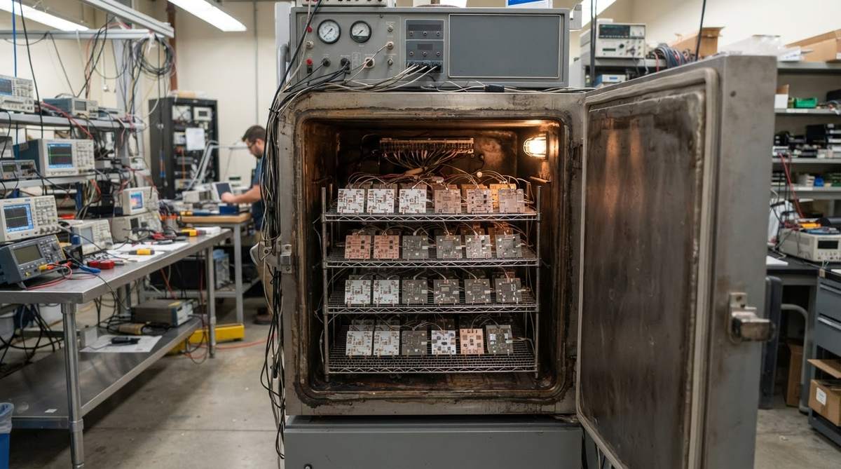
FR-4 is an epoxy-glass composite. Above roughly 130 °C (its Tg), the resin softens, delaminates, and chars. Moisture uptake accelerates copper migration and CAF (conductive anodic filament) growth. Ceramic substrates sidestep all of these mechanisms. Alumina (Al₂O₃ 96%) has no glass transition, absorbs effectively zero moisture, and remains electrically stable to well above 1,000 °C. For an overview of ceramic circuit board fundamentals, the homepage is a good starting point.
Aluminum nitride adds higher thermal conductivity (170–200 W/mK at 25 °C) and a CTE closer to silicon (4.5 ppm/°C), which further reduces thermomechanical stress at die-attach interfaces. If you are evaluating AlN for the first time, the aluminum nitride beginner’s guide covers its properties and trade-offs in detail.
The Five Failure Modes That Actually Limit Ceramic PCB Lifespan
1. Solder-Joint Fatigue from Thermal Cycling
This is the dominant failure mode. Every power-on/power-off cycle imposes a temperature swing (ΔT). The CTE mismatch between the ceramic substrate and the component or heat sink creates shear strain in the solder layer. Over hundreds or thousands of cycles, cracks nucleate at the solder-joint corners and propagate inward until electrical or thermal contact is lost.
The Coffin-Manson relationship governs cycle life. A rough estimate for eutectic SnAgCu (SAC305) solder on an alumina DBC substrate:
Worked example: Assume a 10 × 10 mm die on a 0.635 mm alumina substrate, ΔT = 150 °C, solder thickness 100 µm. The shear strain γ ≈ (ΔT × ΔCTE × L) / (2 × h_solder), where ΔCTE ≈ 11 ppm/°C (copper minus alumina), L = diagonal half-length ≈ 7.07 mm, h_solder = 0.1 mm. γ ≈ (150 × 11 × 10⁻⁶ × 7.07) / (2 × 0.1) ≈ 0.058 (5.8%). Using a Coffin-Manson exponent of −1.9 for SAC305 (per Syed’s model, ECTC 2004), N_f ≈ C × γ^(−1.9). With typical C values, this yields roughly 1,500–2,500 cycles to 50% failure. Switching to a compliant sintered-silver die attach (which tolerates higher strain) can push this past 5,000 cycles.
Choosing the right solder alloy for ceramic boards is one of the highest-leverage decisions for extending service life.
2. Metallization Delamination
Thick-film (screen-printed) metallization bonds to the ceramic through a glass frit phase. If the firing profile is wrong, adhesion can be as low as 3–5 MPa instead of the target 15–25 MPa. DBC (direct bonded copper) relies on a thin CuAlO₂ eutectic layer; contamination or incorrect bonding atmosphere weakens this layer. AMB (active metal brazing) forms a TiN reaction layer on AlN or Si₃N₄ that is more robust but can still crack under extreme thermal shock. For more on AMB substrate construction, see the dedicated explainer.
3. Substrate Cracking from Mechanical Stress
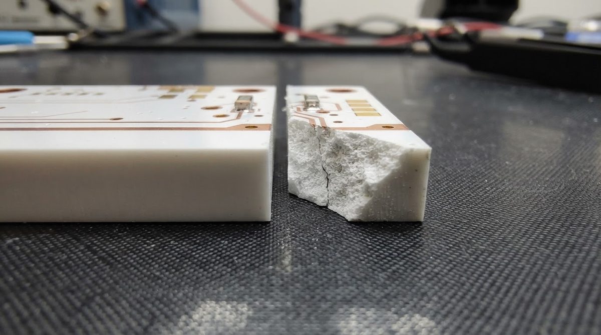
Ceramics are strong in compression but brittle in tension. A ceramic PCB does not bend and spring back like FR-4; it fractures. Common crack sources include over-torqued mounting screws, press-fit connectors, and warped heat sinks that create point loads. Edge chips from handling propagate under thermal cycling. Flexural strength varies significantly by material:
| Material | Flexural Strength (MPa) | Fracture Toughness K_IC (MPa·m^½) | Test Standard | Source |
|---|---|---|---|---|
| Al₂O₃ 96% | 350–380 | 3.5–4.0 | ASTM C1161 | CoorsTek ADS-96R datasheet |
| Al₂O₃ 99.6% | 380–420 | 3.8–4.2 | ASTM C1161 | Kyocera A-493 datasheet |
| AlN | 300–350 | 2.5–3.0 | ASTM C1161 | Maruwa HA-200 datasheet |
| Si₃N₄ | 600–800 | 6.0–7.0 | ASTM C1161 | Kyocera SN-282 datasheet |
Typical values for commercially available material, for comparison only. Confirm against the datasheet for your specific grade.
Si₃N₄ stands out for applications where mechanical shock or vibration is severe, such as EV traction inverters. Its fracture toughness is roughly double that of alumina, meaning it tolerates larger flaws before catastrophic failure.
4. Electromigration and Dendritic Growth
At high DC current densities (above roughly 10⁴ A/cm² in copper traces) and elevated temperatures, copper atoms migrate along grain boundaries, thinning the conductor until it opens. This is the same mechanism that limits IC interconnect life. On ceramic PCBs it is rare because traces are thick (35–300 µm Cu), but it can appear in fine-line DPC metallization running at high current. Ionic migration (dendrite growth) between closely spaced conductors requires both voltage bias and surface moisture. Because ceramic absorbs essentially no water, this mode is far less common than on FR-4, but it can still occur in humid, unconformal-coated assemblies.
5. Environmental Attack on Exposed Metallization
Bare copper oxidizes. In sulfur-rich industrial atmospheres, silver thick-film conductors tarnish and increase in resistance. Proper surface finishes (ENIG, ENEPIG, or gold plating) prevent this, but if the finish is too thin or porous, the underlying metal corrodes over years. Selecting the right finish for the operating environment is essential.
How to Estimate Ceramic PCB Service Life
No single number applies to every design. The substrate itself is not the weak link. Instead, estimate the life of the most stressed interface. For most power-electronics assemblies, that means the solder or sinter layer under the hottest die. Run a Coffin-Manson or Norris-Landzberg calculation using your mission profile’s temperature extremes, ramp rates, and dwell times. Then validate with accelerated thermal-cycling tests per JEDEC JESD22-A104 or IEC 60749-25.
A conservative rule of thumb: if your mission profile imposes fewer than 1,000 full thermal cycles at ΔT ≤ 100 °C over the product’s intended life, a standard DBC or DPC ceramic assembly with SAC305 solder will meet a 20-year target with margin. Higher ΔT, faster ramp rates, or more cycles demand sintered-silver attach, AMB substrates, or Si₃N₄ base material.
Extending Ceramic PCB Lifespan: A Design Checklist
- Minimise CTE mismatch. Match the substrate CTE to the die and heat-sink materials as closely as possible. AlN (4.5 ppm/°C) pairs better with SiC and GaN dies than alumina (6.5–7.0 ppm/°C).
- Use compliant attach materials. Sintered silver or soft solders (e.g., In-based) absorb strain better than rigid SAC305 in high-ΔT applications.
- Avoid point loads at mounting. Use spring clips or compliant thermal interface materials instead of rigid bolted joints. Distribute clamping force over the largest possible area.
- Protect metallization. Specify a surface finish rated for the operating atmosphere and expected shelf time. Proper storage conditions and shelf-life management prevent pre-assembly degradation.
- Control edge quality. Laser-scribed or diamond-sawn edges with a chamfer reduce stress concentrators that initiate cracks.
- Inspect incoming substrates. Reject boards with visible chips or micro-cracks at edges. These grow under thermal cycling.
When a Ceramic PCB Is Not the Right Choice for Longevity
If your product’s service life is under five years and it operates below 100 °C, FR-4 or metal-core PCBs will likely survive the full mission at a fraction of the cost. Ceramic’s lifespan advantage only pays off when temperatures exceed FR-4’s Tg, when the chemical environment attacks organic resins, or when regulatory qualification demands decades of service (aerospace, implantable medical, downhole oil and gas). For a direct comparison of ceramic versus metal-core boards, see the ceramic vs. metal-core decision guide.
Ceramic is also a poor fit for assemblies that will see repeated mechanical impact or flexion. A dropped consumer device, for example, will crack a ceramic board long before an FR-4 board fails.
Frequently Asked Questions
Does a ceramic PCB have a shelf life before assembly?
The bare ceramic substrate does not degrade on the shelf. However, metallized and surface-finished boards can oxidize or absorb contaminants if stored improperly. Vacuum-sealed storage with desiccant in a clean, dry environment preserves solderability for 12 months or more.
Can thermal cycling crack the ceramic itself, not just the solder?
Yes, but it is uncommon in properly designed assemblies. The ceramic cracks when the bonded copper layer exerts enough tensile stress during cooling to exceed the substrate’s fracture strength. This is most likely in DBC with thick copper (≥ 300 µm) on thin alumina (≤ 0.38 mm). Si₃N₄ substrates resist this failure mode far better due to their higher fracture toughness.
How do I test ceramic PCB reliability in the lab?
Accelerated thermal cycling per JEDEC JESD22-A104 (e.g., −40 °C to +150 °C, 1,000 cycles) is the industry standard. Combine it with cross-sectioning and scanning acoustic microscopy (SAM) to detect delamination. Power cycling (active ΔT driven by the device’s own dissipation) is more representative of real field conditions for power modules.
Is a thicker ceramic substrate more durable?
A thicker substrate is stronger in bending (flexural load capacity scales roughly with the square of thickness), but it also increases thermal resistance from junction to heat sink. The optimal thickness balances mechanical robustness against thermal performance. For most power applications, 0.38–0.635 mm is the standard range. See the ceramic PCB thickness options page for available sizes.
What is the end-of-life disposal path for ceramic PCBs?
Ceramic substrates are landfill-inert but the copper and solder contain recoverable metals. Specialised recyclers separate the metallization from the ceramic body, typically by thermal or chemical stripping. The ceramic fraction can be crushed and reused as an abrasive or filler.
Next Step
If you are sizing a ceramic substrate for a long-life application and need material or thickness recommendations, send your mission profile and thermal requirements through the ceramic PCB frequently asked questions page or request a quote directly. An applications engineer can review your thermal-cycle budget and recommend the substrate, metallization, and attach method that meets your target service life.