Aluminum nitride AlN DPC direct plated copper substrates pair a high-thermal-conductivity ceramic (170–230 W/mK) with copper traces deposited by sputtering and electroplating, achieving line/space resolution down to 10 µm. This makes aluminum nitride AlN DPC direct plated copper the go-to substrate for high-power, high-density applications where both heat extraction and circuit precision matter—power semiconductors, laser diodes, RF modules, and LED packages.
Key Takeaways
- AlN DPC substrates achieve thermal conductivity of 170–230 W/mK (per Kyocera and Maruwa datasheets), roughly 7–8× higher than 96% alumina.
- The DPC process produces copper traces with line/space as fine as 10–20 µm, far tighter than DBC’s typical 150 µm minimum.
- Copper thickness in DPC typically ranges from 1 µm to ~100 µm, compared to DBC’s 150–300 µm bonded foil.
- CTE of AlN (4.3–4.7 ppm/°C per CoorsTek SN-AlN datasheet) closely matches silicon (2.6 ppm/°C) and SiC (4.0 ppm/°C), reducing solder-joint fatigue in die-attach applications.
- DPC is more expensive per unit area than DBC but eliminates the high-temperature bonding step that can micro-crack thinner AlN substrates.
What Is the Aluminum Nitride AlN DPC Direct Plated Copper Process?
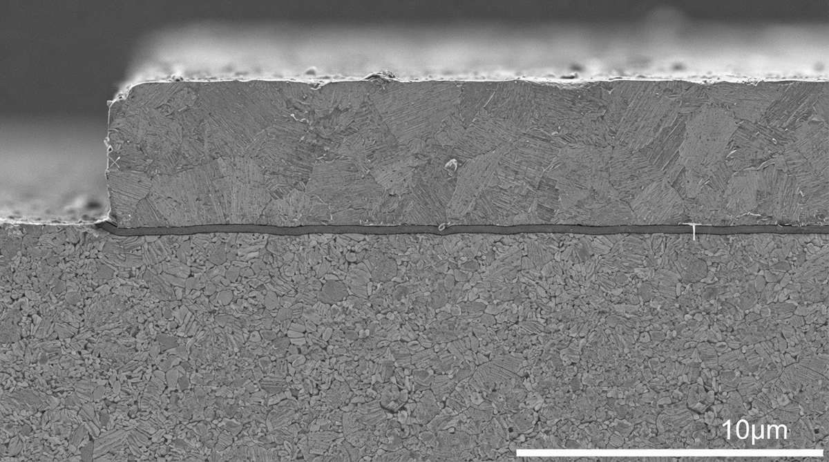
DPC stands for direct plated copper. It is an additive metallization method, distinct from the oxide-eutectic bonding used in DBC (direct bonded copper). The process sequence on an aluminum nitride substrate is:
- Substrate cleaning and surface prep. The AlN ceramic is ultrasonically cleaned and plasma-treated to improve adhesion.
- Sputtering of an adhesion/seed layer. A thin titanium (Ti) or chromium (Cr) layer (~50–200 nm) is sputtered onto the ceramic, followed by a copper seed layer (~200–500 nm).
- Photolithography. Photoresist is applied, exposed through a mask, and developed to define the circuit pattern.
- Copper electroplating. Copper is electroplated into the open resist areas to the target thickness (typically 10–100 µm).
- Resist strip and seed etch. The photoresist is stripped, and the exposed seed/adhesion layers are etched away, leaving isolated copper traces on AlN.
Because the copper is built up from a sputtered seed rather than bonded as a thick foil, the aluminum nitride AlN DPC direct plated copper process avoids the 1,065 °C Cu-O eutectic temperatures needed for DBC. This matters for AlN: the substrate’s surface can oxidize above ~700 °C in air, degrading thermal performance. DPC processing stays well below that threshold.
For a broader look at how ceramic circuit boards move from raw material to finished product, see the ceramic PCB manufacturing process overview.
AlN DPC Material and Performance Specifications
| Parameter | Value | Unit | Condition | Source |
|---|---|---|---|---|
| Thermal conductivity (AlN) | 170–230 | W/mK | 20 °C, varies by grain size and oxygen content | Kyocera SN-AlN / Maruwa HA-230 |
| Dielectric strength | 15–17 | kV/mm | AC, 1 mm thick, per ASTM D149 | CoorsTek AlN datasheet |
| CTE | 4.3–4.7 | ppm/°C | 20–400 °C | CoorsTek / Kyocera |
| Flexural strength | 300–400 | MPa | 3-point bend, per ASTM C1161 | Kyocera SN-AlN |
| Copper thickness (DPC) | 1–100 | µm | Electroplated | Industry typical |
| Min line/space (DPC) | 10–20 | µm | Photolithographic process | Industry typical |
| Surface roughness (Ra, AlN) | 0.1–0.5 | µm | Lapped or as-fired, grade dependent | Maruwa HA series |
Typical values for commercially available material, for comparison only. Confirm against the datasheet for your specific grade.
The thermal conductivity of AlN is highly sensitive to oxygen impurity levels. Grades with <1% oxygen content routinely reach 200+ W/mK, while lower-purity grades may sit closer to 170 W/mK. For a deeper discussion, see aluminum nitride thermal conductivity explained.
Aluminum Nitride AlN DPC Direct Plated Copper vs. DBC vs. Thin Film
| Parameter | DPC | DBC | Thin Film |
|---|---|---|---|
| Min line/space | 10–20 µm | 150–200 µm | 5–15 µm |
| Copper thickness | 1–100 µm | 150–300 µm | 0.5–5 µm |
| Current carrying capacity | Moderate | High (thick Cu) | Low |
| Bond temperature | <100 °C (plating bath) | ~1,065 °C (Cu-O eutectic) | <300 °C (sputter/evaporate) |
| Thermal cycling reliability | Good (thin Cu, low stress) | Good (but Cu-ceramic CTE stress) | Excellent (very thin metal) |
| Relative cost per unit area | High | Moderate | Very high |
Choose aluminum nitride AlN DPC direct plated copper when you need fine features (≤50 µm traces) with moderate current handling—laser submounts, MMIC carriers, high-brightness LED arrays. Choose DBC when you need thick copper for high-current power modules (IGBTs, SiC MOSFETs) and fine lines are not critical. Choose thin film when you need the tightest tolerances and lowest parasitics, as in mmWave RF circuits, and current is minimal.
If your application demands even higher thermal-cycling endurance at the cost of thermal conductivity, consider silicon nitride DBC substrates, which offer superior mechanical toughness (flexural strength >600 MPa) though lower thermal conductivity (70–90 W/mK).
For thin-film metallization on AlN, AlN thin film substrates cover the process and design rules in detail.
Worked Example: Thermal Resistance of an AlN DPC Substrate
Estimate the conduction thermal resistance (Rth) through a 0.635 mm thick AlN DPC substrate with a 10 mm × 10 mm footprint and thermal conductivity of 200 W/mK:
Rth = t / (k × A)
Rth = 0.000635 m / (200 W/mK × 0.0001 m²) = 0.032 °C/W
For comparison, the same geometry in 96% alumina (k = 25 W/mK) gives Rth = 0.254 °C/W—about 8× higher. At 50 W dissipation, the AlN substrate adds only 1.6 °C to the thermal stack, versus 12.7 °C for alumina. That difference can eliminate a forced-air heatsink or allow a smaller package.
Enter your substrate dimensions, thickness, and dissipated power below to estimate junction temperature rise for your own aluminum nitride AlN DPC direct plated copper design.
For guidance on optimizing your full thermal stack, see the AlN thermal design guide.
Design Considerations for AlN DPC Substrates
Substrate Thickness
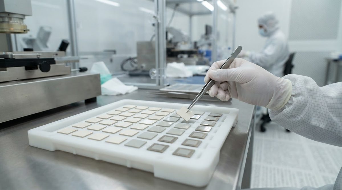
Common AlN DPC substrate thicknesses are 0.25 mm, 0.385 mm, 0.635 mm, and 1.0 mm. Thinner substrates reduce thermal resistance but are more fragile during handling and assembly. For substrates below 0.385 mm, specify vacuum pick-and-place tooling and avoid mechanical clamping.
Copper Adhesion
The sputtered Ti or Cr adhesion layer is critical. Peel strength for well-processed DPC copper on AlN is typically 4–8 N/mm (per IPC-TM-650 method 2.4.8). If you see values below 3 N/mm, suspect contamination or insufficient plasma pre-treatment.
Surface Finish
After copper patterning, DPC substrates are typically finished with electroless nickel / immersion gold (ENIG), electrolytic Ni/Au, or Ag plating depending on the die-attach method. For AuSn eutectic die attach (common in laser diodes), electrolytic Au of 1–3 µm over 3–5 µm Ni is standard.
When Not to Use AlN DPC
High-current power modules (>100 A). DPC copper tops out around 100 µm. If you need 200+ µm copper for bus bars or high-current traces, DBC on AlN or AMB on Si₃N₄ is the better path.
Cost-sensitive, low-power designs. If thermal conductivity above 25 W/mK is sufficient and feature sizes are >100 µm, 96% alumina with thick-film metallization costs a fraction of AlN DPC. Do not over-specify the substrate.
Very large panels. AlN substrates are typically available up to about 114 mm × 114 mm (4.5″ × 4.5″). If your design requires larger single-piece substrates, alumina or Si₃N₄ may offer better availability.
Extreme mechanical shock. AlN flexural strength (300–400 MPa) is adequate for most electronics, but Si₃N₄ (>600 MPa, per Kyocera SN-Si₃N₄ datasheet) is more forgiving in automotive under-hood or downhole environments.
Frequently Asked Questions
Can you solder directly to AlN DPC copper?
Yes. The electroplated copper surface accepts standard soldering processes—reflow, wave, and manual—provided the surface finish is appropriate. ENIG or electrolytic Ni/Au are the most common finishes for solderability. Bare copper will oxidize and should be finished within hours of final etch.
Does DPC copper delaminate during thermal cycling?
Well-processed DPC substrates with a proper Ti/Cu adhesion layer survive >1,000 cycles from −40 °C to +150 °C without delamination, per MIL-STD-883 Method 1010 style testing. The thin copper layer generates less CTE-mismatch stress than the 200–300 µm foil in DBC, so DPC often has an edge in cycling endurance.
What is the maximum operating temperature for AlN DPC?
The AlN ceramic itself is stable above 1,000 °C in inert atmosphere. The practical limit is set by the copper metallization and solder joints: continuous operation up to 350–400 °C is feasible with appropriate high-temperature solders (e.g., AuSn, AuGe). Standard SnAgCu solder limits continuous use to about 150 °C. For more on high-temperature operation, see AlN at high temperature and power.
How thin can the AlN substrate be for DPC?
AlN substrates as thin as 0.25 mm (250 µm) are routinely used for DPC. Below 0.25 mm, yields drop due to handling breakage and warpage during sputtering. For most power applications, 0.385 mm or 0.635 mm offers the best balance of thermal resistance and mechanical robustness.
Is AlN DPC suitable for RF and microwave circuits?
Yes, for applications up to roughly 20–30 GHz. AlN’s dielectric constant is 8.5–9.0 at 1 MHz (per Kyocera datasheet), and DPC’s fine-line capability supports 50 Ω microstrip and coplanar waveguide geometries. Above 40 GHz, thin-film metallization on AlN or quartz substrates gives tighter impedance control.
Next Step
If you are evaluating aluminum nitride AlN DPC direct plated copper for a specific design, start by confirming your required trace width, copper thickness, and thermal budget against the specifications above. Request a sample kit to verify solderability and die-attach compatibility with your assembly process before committing to production volumes.