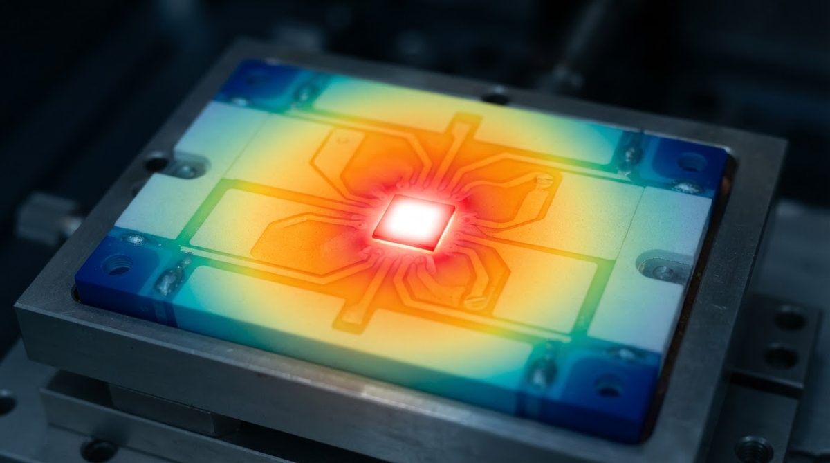
Aluminum nitride AlN thermal design starts with one number: 170–230 W/mK thermal conductivity at 25 °C, roughly 6–8× higher than 96% alumina. That single property makes AlN the default ceramic substrate for high-power-density electronics where junction temperature is the binding constraint. But conductivity alone does not guarantee a good thermal design. Substrate thickness, metallization method, die-attach material, and CTE matching all interact, and getting any one wrong can erase the advantage you paid for.
Why AlN Matters for Thermal Design
AlN combines high thermal conductivity with a coefficient of thermal expansion (CTE) of 4.4–4.7 ppm/°C, close to silicon (2.6 ppm/°C), GaN-on-SiC (4.2 ppm/°C), and SiC (4.0 ppm/°C). That match reduces thermomechanical stress at the die-attach joint during power cycling, which directly extends solder-joint fatigue life. For comparison, a standard alumina substrate at 7.2 ppm/°C creates roughly 60–70% more CTE mismatch against a SiC die.
AlN also maintains a dielectric strength above 15 kV/mm (per ASTM D149) and volume resistivity above 10¹³ Ω·cm, so it functions as both a heat spreader and an electrical insulator in a single layer. This dual role eliminates the need for separate insulating pads in power modules, simplifying the stack and removing one thermal interface. For a broader look at high thermal conductivity PCB options, including DBC and AMB on alumina, see the comparison page.
Key Material Properties for Aluminum Nitride AlN Thermal Design
| Parameter | Value | Unit | Condition | Source |
|---|---|---|---|---|
| Thermal conductivity | 170–230 | W/mK | 25 °C, varies by purity/grain size | Kyocera SH-30 / Maruwa AN-230 datasheets |
| CTE | 4.4–4.7 | ppm/°C | 25–400 °C | CoorsTek ADS-996 |
| Dielectric strength | 15–17 | kV/mm | ASTM D149, 1 mm thick | Maruwa AN-230 |
| Flexural strength | 300–400 | MPa | ASTM C1161, 3-pt bend | Kyocera SH-30 |
| Volume resistivity | >10¹³ | Ω·cm | 25 °C | CoorsTek ADS-996 |
| Max continuous use temp | 1000 | °C | In inert/vacuum; 700 °C in air (oxidation limit) | CeramTec Alunit |
Typical values for commercially available material, for comparison only. Confirm against the datasheet for your specific grade.
The wide conductivity range (170–230 W/mK) reflects real grade differences. A 170 W/mK substrate costs significantly less than a 230 W/mK one. For many designs, 170 W/mK is more than adequate. Run the thermal math before specifying the premium grade. For temperature limits of ceramic substrates in general, see what temperature ceramic PCBs can handle.
Worked Example: Thermal Resistance in an AlN Thermal Design
Thermal resistance (Rth) through the substrate itself is straightforward to estimate for a first-pass aluminum nitride AlN thermal design:
Rth = t / (k × A)
Where t = substrate thickness, k = thermal conductivity, A = heat-spreading area under the die.
Scenario: A GaN HEMT dissipates 50 W through a 5 mm × 5 mm footprint on a 0.635 mm thick AlN substrate (k = 180 W/mK).
- t = 0.000635 m
- A = 0.005 × 0.005 = 2.5 × 10⁻⁵ m²
- Rth,substrate = 0.000635 / (180 × 2.5 × 10⁻⁵) = 0.141 °C/W
- ΔT across substrate = 50 W × 0.141 °C/W = 7.1 °C
The same geometry on 96% alumina (k = 25 W/mK) gives Rth = 1.016 °C/W and ΔT = 50.8 °C. That 43.7 °C difference is why AlN exists as a product. For a deeper walkthrough of the math, including interface layers, see ceramic PCB thermal resistance calculations.
Note: this 1-D estimate ignores lateral spreading, which is significant when the substrate is much larger than the die. A 2-D or FEA model will show a lower effective Rth because heat fans out before reaching the bottom surface. Set up your FEA boundary conditions correctly using the thermal simulation guide for ceramic boards.
Enter your substrate area, thickness, and dissipated power below to estimate junction temperature rise for your own aluminum nitride AlN thermal design scenario.
Layout and Stack-Up Rules for AlN Boards
Substrate Thickness
Thinner substrates reduce Rth linearly but are more fragile and harder to handle during assembly. Common AlN thicknesses are 0.25 mm, 0.38 mm, and 0.635 mm. For single-die power stages under 100 W, 0.38 mm is a practical starting point. Below 0.25 mm, yield loss during metallization and assembly rises sharply.
Metallization Choice
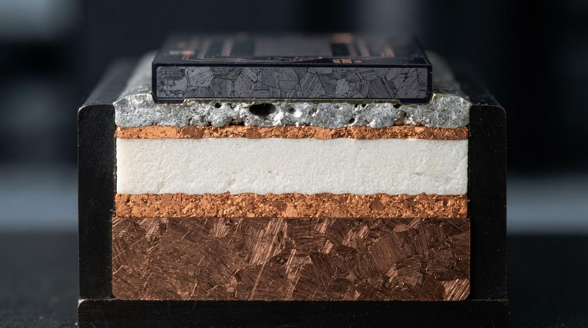
AlN substrates are typically metallized by DBC (direct bond copper), AMB (active metal brazing), or thin-film sputtering (Ti/Pt/Au or Ti/Ni/Au). DBC on AlN is less mature than DBC on alumina because AlN requires an oxidation pre-treatment to form a bonding oxide layer; AMB avoids this step and produces a stronger bond. For high-reliability power modules (automotive inverters, traction drives), AMB on AlN is the dominant choice. Thin-film metallization suits RF and microwave applications where trace geometry tolerances under 25 µm matter.
Die Attach
The die-attach layer is often the largest single thermal resistance in the stack. AuSn (80/20) solder gives a bond-line thermal conductivity of ~57 W/mK at 20–30 µm thickness. Sintered silver paste reaches 150–250 W/mK at similar thickness and survives higher operating temperatures, but requires pressure sintering equipment and careful process control. For a 50 W die on a 5 × 5 mm pad, switching from AuSn to sintered Ag can save 0.5–1.5 °C at the junction.
Heat Spreader Integration
If junction-to-ambient Rth is still too high after optimizing the substrate, adding a copper or CuMo heat spreader below the AlN can help. The CTE of pure copper (17 ppm/°C) is a poor match to AlN (4.5 ppm/°C), so CuMo (CTE ~7–8 ppm/°C) or AlSiC composites are preferred for power-cycling reliability. For design guidance on spreader sizing and attachment, see the ceramic heat spreader design page.
When NOT to Use AlN
Cost-sensitive, moderate-power designs. AlN substrates cost 3–5× more per unit area than 96% alumina. If your die dissipates under 10 W over a reasonable footprint and junction temperature has margin, alumina or even a metal-core PCB (MCPCB) will work at a fraction of the price.
Large board areas. AlN is practical up to roughly 50 × 50 mm per substrate. Larger panels are available but expensive and prone to warpage. If your circuit requires a 100 × 100 mm board with modest thermal demands, FR-4 or alumina is more sensible.
Mechanical shock environments without proper mounting. AlN has good flexural strength (300–400 MPa) but zero ductility. A direct mechanical mount with no compliant interface will crack the substrate under vibration or shock. If your application involves severe mechanical loads and you need ceramic, silicon nitride with its superior fracture toughness may be a better fit.
Humid, unprotected environments. AlN hydrolyzes slowly in the presence of moisture, degrading surface conductivity over time. Passivation coatings or hermetic packaging are required for long-term reliability in humid conditions.
Frequently Asked Questions
Does AlN thermal conductivity drop at high temperatures?
Yes. AlN thermal conductivity decreases with temperature, falling to roughly 100–140 W/mK at 300 °C depending on grade. Always use the conductivity value at your expected operating temperature, not the room-temperature spec. Kyocera and Maruwa datasheets publish conductivity vs. temperature curves for each grade.
Can I use standard SAC305 solder on AlN?
SAC305 wets properly metallized AlN surfaces (Ni/Au or Ni/Pd/Au finish) without issue. The concern is not wettability but CTE mismatch fatigue over thermal cycles. For high-reliability applications, AuSn or sintered silver is preferred over SAC305 because both tolerate more power cycles before joint failure.
Is AlN safe to handle and machine?
AlN dust is an irritant but not classified as a carcinogen. Standard ceramic dust controls apply: use wet machining or vacuum extraction, and wear a particulate respirator when grinding or laser-scribing. Unlike beryllium oxide, AlN does not require a hazardous-material handling program.
How does aluminum nitride AlN thermal design compare to Si₃N₄?
AlN wins on thermal conductivity (170–230 vs. 70–90 W/mK for Si₃N₄). Si₃N₄ wins on mechanical toughness (fracture toughness ~6.5 MPa·√m vs. ~2.5–3.5 for AlN). For applications dominated by thermal cycling fatigue, such as automotive traction inverters, Si₃N₄ AMB substrates are increasingly preferred despite the conductivity penalty.
What is the thinnest AlN substrate available?
Standard catalog thicknesses go down to 0.25 mm (250 µm). Some suppliers offer 0.15 mm for specialty RF and laser-diode submounts, but handling and metallization yield at that thickness require tight process control.