Thermal simulation PCB work on ceramic substrates requires accurate material properties, correct boundary conditions, and a mesh fine enough to capture thin copper and substrate layers without blowing up solve time. Get any one of those wrong and your predicted junction temperature can drift 15–30 °C from reality. This guide walks through each setup step for finite-element and computational-fluid-dynamics tools commonly used with alumina, aluminum nitride, and silicon nitride substrates.
Key Takeaways
- Ceramic thermal conductivity is temperature-dependent: AlN drops from ~170 W/mK at 25 °C to ~120 W/mK at 300 °C (per Kyocera SH-30 datasheet). Enter a single room-temperature value and you will under-predict hot-spot temperatures.
- Interface thermal resistance (TIM layers, solder joints, die-attach) often dominates the total Rth more than the substrate itself. Model every interface explicitly.
- A minimum of three elements through the substrate thickness is needed to resolve the temperature gradient; five or more is preferred for substrates thinner than 0.38 mm.
- Convection coefficients on exposed ceramic surfaces are typically 5–15 W/m²K for natural convection and 25–100 W/m²K for forced air, per JEDEC JESD51-12.
- Validate simulation against a thermal test coupon before trusting results on a production layout.
Why Ceramic Substrates Need a Dedicated Thermal Simulation PCB Approach
FR-4 thermal simulation is forgiving because the substrate’s conductivity is so low (0.25–0.35 W/mK) that nearly all heat flows through copper planes and vias. In a ceramic PCB, the substrate itself carries a significant share of the heat. A 96 % alumina board conducts 24–28 W/mK, and an AlN board conducts 170–200 W/mK. That means the substrate’s in-plane and through-plane conduction must be modeled with real geometry, not lumped into an effective conductivity the way many engineers treat FR-4 cores.
Ceramic substrates are also used in environments where temperature swings are large: power modules cycling from ambient to 150 °C+, LED arrays running at 85 °C board temperature, and RF amplifiers dissipating tens of watts per square centimetre. Temperature-dependent properties matter here far more than in a consumer electronics board sitting at 40 °C. For a full comparison of ceramic PCB substrate materials, including thermal conductivity ranges and CTE values, start with actual datasheet numbers rather than textbook generalisations.
Material Property Inputs for Thermal Simulation PCB Models
Every solver needs at minimum: thermal conductivity (k), density (ρ), and specific heat capacity (Cp) for each material in the stack. For steady-state analysis you can skip ρ and Cp, but most real-world problems involve transient loads, so enter all three.
| Material | k (W/mK) at 25 °C | k (W/mK) at 300 °C | ρ (g/cm³) | Cp (J/gK) | Source |
|---|---|---|---|---|---|
| Al₂O₃ 96 % | 24–28 | 14–18 | 3.72 | 0.78 | CoorsTek ADS-96R datasheet |
| Al₂O₃ 99.6 % | 30–35 | 18–22 | 3.89 | 0.78 | Kyocera A-493 datasheet |
| AlN | 170–200 | 120–140 | 3.26 | 0.74 | Kyocera SH-30 datasheet |
| Si₃N₄ | 70–90 | 55–70 | 3.20 | 0.68 | Kyocera SN-90 datasheet |
| Cu (electroplated) | 385–395 | 370–380 | 8.96 | 0.39 | ASTM E1225 |
| SAC305 solder | 58–62 | 52–56 | 7.37 | 0.23 | NIST solder database |
Typical values for commercially available material, for comparison only. Confirm against the datasheet for your specific grade.
Enter k as a piecewise-linear function of temperature, not a constant. In ANSYS Mechanical, use the “Tabular” input under Engineering Data; in COMSOL, use an interpolation function. If your solver only accepts a single value, pick the conductivity at the expected average substrate temperature, not the room-temperature value. Accurate thermal simulation PCB results depend on this step more than any other single input.
Interface Layers You Must Not Skip
Die-attach epoxy or solder, TIM pads, and the bond between a DBC copper layer and the ceramic core each add thermal resistance. A typical Ag-filled die-attach epoxy has k ≈ 1.5–3 W/mK at a bondline thickness of 25–50 µm. That thin layer alone can contribute 0.5–1.5 °C/W to the total path. Model it as a solid layer with its own mesh, or as a thermal contact resistance (Rth,interface = t / k × A) applied at the interface. The copper plating capabilities and tolerances of your fabricator determine the actual copper thickness in the model, so use measured values from a cross-section if available.
Meshing Strategy for Thin-Layer Ceramic Stacks
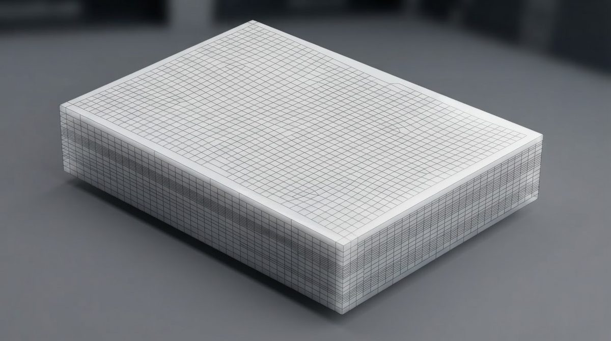
A ceramic substrate is often 0.25–1.0 mm thick, with copper layers of 0.035–0.30 mm on each side. If you auto-mesh with tetrahedral elements, the solver will either create millions of tiny elements or produce a coarse mesh that misses the through-thickness gradient entirely.
Use swept (hex) meshing for each planar layer. Set a minimum of three elements through the substrate thickness and two elements through each copper layer. For a 0.635 mm alumina substrate, that means element edges of ~0.21 mm or smaller in the z-direction. In-plane element size can be 5–10× larger where the heat flux is uniform, but refine to 0.1–0.2 mm around die-attach pads and thermal via arrays for heat dissipation.
Mesh Convergence Check
Run three mesh densities: coarse, baseline, and fine (double the element count each time). If the peak temperature changes by less than 1 °C between baseline and fine, baseline is adequate. Document the convergence in your report. Skipping this step is the most common reason thermal simulation PCB predictions and physical measurements disagree.
Boundary Conditions That Match Reality
The boundary conditions you apply to the model’s outer surfaces control where heat leaves the system. Common setups:
- Fixed-temperature base. If the ceramic board is soldered to a copper heat spreader on a liquid-cooled cold plate, set the bottom surface to the cold-plate temperature (e.g., 25 °C or 65 °C). This is the simplest and most repeatable boundary.
- Convection on exposed surfaces. Apply a convection coefficient (h) and ambient temperature. For natural convection in still air, h = 5–15 W/m²K is typical for a small horizontal board (per JEDEC JESD51-12). For forced air at 1–3 m/s, h = 25–60 W/m²K. Over-estimating h by even 2× will under-predict your hot-spot by 10–20 °C.
- Radiation. At board temperatures above 100 °C, radiation becomes non-trivial. Ceramic emissivity is 0.85–0.95 for unglazed alumina. Include surface-to-ambient radiation for any exposed ceramic face in high-temperature applications. For more on the maximum operating temperature limits of ceramic substrates, the upper bound is set by metallisation and solder, not the ceramic itself.
Enter your substrate dimensions, layer thicknesses, and power dissipation below to estimate the temperature rise through your ceramic stack and check whether your boundary assumptions are reasonable.
Worked Example: 10 W GaN Die on AlN DBC
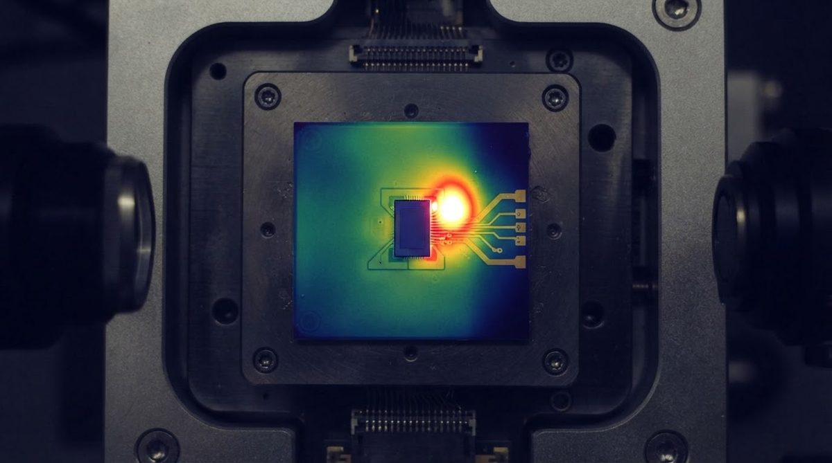
Consider a 3 mm × 3 mm GaN HEMT dissipating 10 W, mounted on an AlN DBC substrate (0.635 mm AlN, 0.30 mm Cu top and bottom), soldered to a copper base plate held at 25 °C.
Step 1 — Conduction through die-attach. SAC305 solder, 50 µm thick, area = 9 mm².
Rth,solder = t / (k × A) = 0.00005 / (60 × 9 × 10⁻⁶) = 0.093 °C/W.
Step 2 — Conduction through top Cu. 0.30 mm thick. Heat spreading widens the effective area to roughly 5 mm × 5 mm = 25 mm².
Rth,Cu_top = 0.0003 / (390 × 25 × 10⁻⁶) = 0.031 °C/W.
Step 3 — Conduction through AlN. 0.635 mm thick, spreading area ~7 mm × 7 mm = 49 mm².
Rth,AlN = 0.000635 / (180 × 49 × 10⁻⁶) = 0.072 °C/W.
Step 4 — Conduction through bottom Cu and solder to base plate. Similar calculation yields ~0.05 °C/W combined.
Total Rth ≈ 0.093 + 0.031 + 0.072 + 0.05 = 0.246 °C/W.
ΔT = 10 W × 0.246 °C/W = 2.46 °C. Predicted junction temperature ≈ 27.5 °C above the base plate.
A 3-D FEA model of the same geometry typically returns 2.2–2.8 °C rise, confirming the hand calculation is in the right range. The discrepancy comes from heat-spreading geometry that the 1-D calculation approximates. This cross-check is essential before trusting any complex thermal simulation PCB model. For the underlying math, see the guide on ceramic thermal management and Rth calculations.
Common Thermal Simulation PCB Mistakes
- Using isotropic copper for DBC. Electroplated and rolled copper have nearly identical k, but DBC copper grain structure can differ. Use the datasheet value from the DBC supplier, not generic OFHC copper.
- Ignoring the ceramic-to-copper bond layer. In DBC, the oxide interlayer is ~1–5 µm and has k ≈ 10–30 W/mK. At high power densities this adds measurable resistance.
- Applying symmetry incorrectly. Symmetry planes must have zero heat flux across them. If your layout is not truly symmetric (different trace widths on left vs. right), do not cut the model in half.
- Omitting the multilayer ceramic build-up in LTCC or HTCC designs. Each co-fired layer may have slightly different porosity and k. Model each layer individually.
When Not to Use Detailed Ceramic Thermal Simulation
If your board dissipates less than 1 W total and operates below 85 °C, a simple 1-D Rth hand calculation is usually sufficient. The effort of building a 3-D FEA model is not justified when the temperature rise is only a few degrees and the design margin is large.
Similarly, if you are using standard FR-4 or metal-core PCB with well-characterised thermal vias, most solver vendors provide built-in PCB models (e.g., Ansys Icepak’s “PCB block” model) that handle the effective conductivity automatically. Detailed layer-by-layer modelling is most valuable for ceramic substrates because their high conductivity makes the substrate geometry matter.
FAQ
Which solver should I use for ceramic PCB thermal simulation?
ANSYS Mechanical, COMSOL Multiphysics, and Siemens Simcenter Flotherm all handle ceramic substrates well. The choice depends on your licence availability and whether you need conjugate heat transfer (airflow + conduction) or conduction-only analysis. For conduction-only steady-state, even a free tool like Elmer FEM works.
Do I need to model the ceramic substrate as anisotropic?
No. Polycrystalline alumina, AlN, and Si₃N₄ are thermally isotropic. Their grain orientation is random after sintering. Use a single k value (or temperature-dependent curve) for all directions.
How do I get the thermal conductivity of my specific ceramic grade?
Request the datasheet from the substrate manufacturer (CoorsTek, Kyocera, Maruwa, or CeramTec). The k value is measured per ASTM E1461 (laser flash method) and reported at 25 °C. Ask for the temperature-dependent curve if your operating range exceeds 100 °C.
Can I validate the simulation without a thermal test vehicle?
You can do a rough check by measuring the board’s surface temperature with an IR camera or thermocouple under known power input. However, a purpose-built thermal test vehicle with embedded diode temperature sensors, per JEDEC JESD51-1, gives the most reliable Rth measurement for correlation.
How accurate is a 1-D Rth calculation compared to 3-D FEA?
A 1-D calculation typically agrees within ±15–25 % of a 3-D FEA result for single-die layouts. The error grows with multiple heat sources, non-uniform copper patterns, or when lateral spreading is significant relative to the substrate area. Use 1-D for initial sizing and 3-D for final design verification.