A high thermal conductivity PCB uses a substrate material that moves heat away from components faster than standard FR-4, which conducts only 0.3–0.4 W/mK through the board thickness. Ceramic substrates offer 24–200 W/mK depending on grade, while metal-core PCBs (MCPCBs) reach 1–4 W/mK through their dielectric layer. Choosing the right option depends on your power density, maximum junction temperature, and budget.
Key Takeaways
- 96% alumina (Al₂O₃) provides 24–28 W/mK at 20 °C and is the most cost-effective ceramic substrate for moderate thermal loads.
- Aluminum nitride (AlN) reaches 170–200 W/mK at 20 °C, roughly 6–8× higher than 96% alumina, but costs 3–5× more per unit area.
- Silicon nitride (Si₃N₄) offers 70–90 W/mK with the highest fracture toughness of any engineering ceramic, making it the choice for power modules under thermal cycling.
- Metal-core PCBs are cheaper than ceramics but limited to 1–4 W/mK through the dielectric; they suit LED arrays and low-density power boards, not high-flux devices.
- FR-4 thermal conductivity is roughly 500× lower than AlN—no amount of copper planes or thermal vias closes that gap for high-power-density designs.
Why Substrate Thermal Conductivity Matters for Your Design
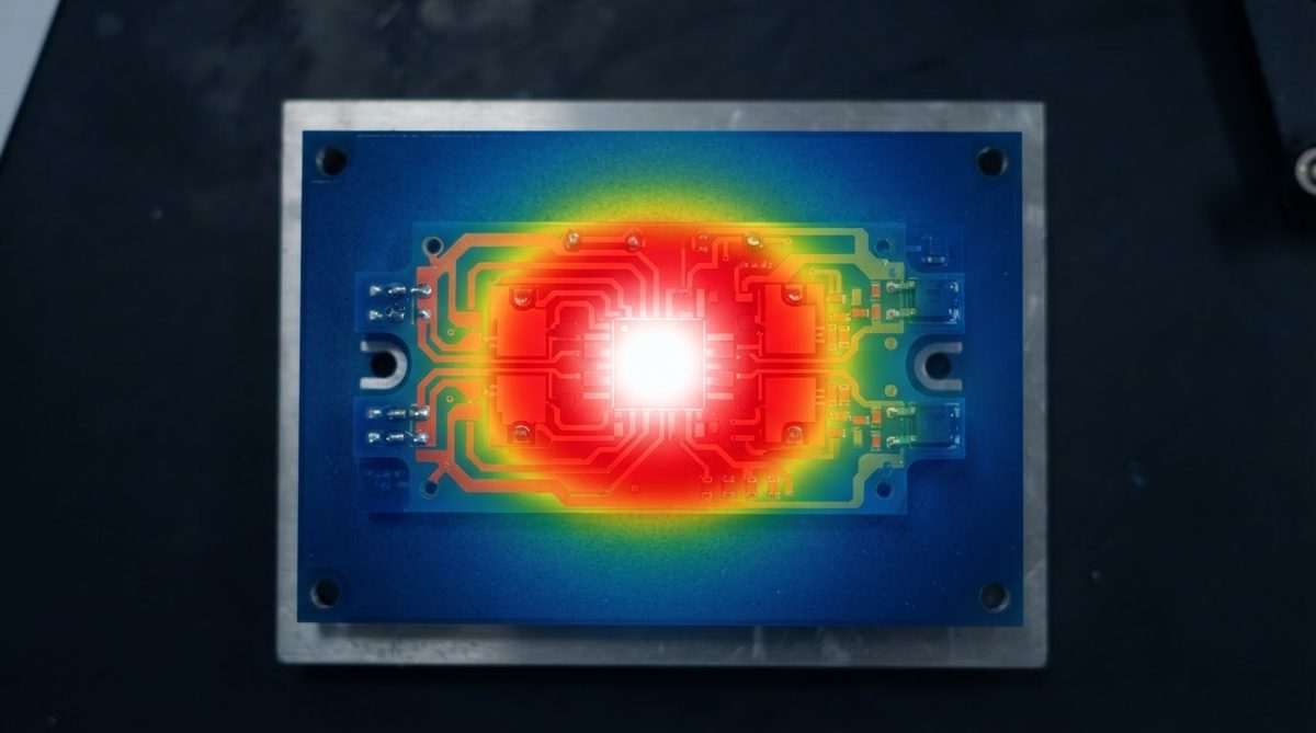
The substrate sits directly in the heat path between a die or component and the heatsink. Its thermal resistance is proportional to thickness and inversely proportional to thermal conductivity and area. A substrate with higher thermal conductivity reduces the temperature drop across the board, which directly lowers junction temperature.
For a simple one-dimensional estimate, the thermal resistance through the substrate is:
Rth = t / (k × A)
where t is substrate thickness (m), k is thermal conductivity (W/mK), and A is the heat-spreading area (m²). You can estimate the Rth of a ceramic substrate stack with this formula as a starting point, then refine with FEA for real geometries.
Comparing High Thermal Conductivity PCB Substrates
The table below summarizes the main substrate families used in thermally demanding electronics. All values are for commercially available grades at room temperature unless noted.
| Substrate | Thermal Conductivity (W/mK) | Dielectric Strength (kV/mm) | CTE (ppm/°C) | Relative Cost | Source |
|---|---|---|---|---|---|
| FR-4 (glass-epoxy) | 0.3–0.4 | 20–30 | 14–17 (x/y) | 1× | IPC-4101E |
| MCPCB dielectric layer | 1–4 | 3–6 | N/A (aluminum base ~23) | 2–4× | Bergquist / Henkel datasheets |
| Al₂O₃ 96% | 24–28 | 10–15 | 7.1 | 8–15× | CoorsTek ADS-96R datasheet |
| Al₂O₃ 99.6% | 30–35 | 12–17 | 7.4 | 15–25× | Kyocera A-493 datasheet |
| Si₃N₄ | 70–90 | 15–20 | 2.7 | 30–50× | Kyocera SN-282 datasheet |
| AlN | 170–200 | 15–17 | 4.5 | 40–70× | Maruwa HA-200 datasheet |
Typical values for commercially available material, for comparison only. Confirm against the datasheet for your specific grade.
For a deeper comparison of these ceramic grades, see the full ceramic PCB material selection guide.
Worked Example: Junction Temperature Drop Across Substrates
Consider a GaN HEMT dissipating 50 W through a 10 mm × 10 mm footprint on a 0.635 mm thick substrate. We compare the substrate-only thermal resistance for three ceramics:
96% Al₂O₃ (k = 26 W/mK):
Rth = 0.000635 / (26 × 0.0001) = 0.244 °C/W → ΔT = 50 × 0.244 = 12.2 °C
Si₃N₄ (k = 80 W/mK):
Rth = 0.000635 / (80 × 0.0001) = 0.079 °C/W → ΔT = 50 × 0.079 = 4.0 °C
AlN (k = 180 W/mK):
Rth = 0.000635 / (180 × 0.0001) = 0.035 °C/W → ΔT = 50 × 0.035 = 1.8 °C
The difference between alumina and AlN is about 10 °C at the substrate alone. In a real assembly, this margin compounds with interface layers and heatsink resistance. For devices where junction temperature is already near the 150–175 °C limit, that 10 °C is the difference between passing and failing qualification. Run a thermal simulation of your ceramic board to capture spreading effects that the 1-D formula misses.
When to Use Each Substrate
96% Alumina: The Workhorse
Alumina at 96% purity is the default ceramic PCB substrate. It handles most power LED, sensor, and RF applications where FR-4 falls short but the heat flux stays below roughly 30–50 W/cm². It is widely available, compatible with thick-film, thin-film, DPC, and HTCC/LTCC processes, and its CTE of 7.1 ppm/°C is a reasonable match for silicon (2.6 ppm/°C) and GaAs (5.7 ppm/°C). Choosing alumina keeps substrate cost at roughly one-tenth the price of AlN.
99.6% Alumina: A Modest Step Up
Moving from 96% to 99.6% alumina raises thermal conductivity from ~26 to ~32 W/mK—a 20–25% improvement. The glass phase is nearly eliminated, which also improves high-frequency dielectric loss. This grade makes sense for RF power amplifiers and precision thin-film circuits where the extra cost is justified by tighter property control.
Aluminum Nitride: Maximum Thermal Performance
AlN is the highest thermal conductivity ceramic substrate in common production. At 170–200 W/mK, it approaches copper’s conductivity while remaining an electrical insulator. Its CTE of 4.5 ppm/°C is the closest match to silicon among all ceramic substrates. The trade-off is cost: AlN substrates run 3–5× more than equivalent alumina parts, and the material is harder to machine. Use AlN for IGBT modules, high-power laser diodes, GaN/SiC power devices, and any application where the thermal budget has no room left.
Silicon Nitride: Toughness Under Thermal Cycling
Si₃N₄ substrates offer silicon nitride thermal conductivity of 70–90 W/mK, lower than AlN but paired with fracture toughness of 6–7 MPa·m½ (per Kyocera SN-282 datasheet, ASTM C1421). That is roughly 3× tougher than AlN. For EV traction inverters and railway power modules that endure thousands of deep thermal cycles (ΔT > 150 °C), Si₃N₄ AMB substrates survive where AlN cracks. The material’s low CTE of 2.7 ppm/°C also reduces stress on bonded copper layers.
Metal-Core PCBs vs. Ceramic: A Common Comparison
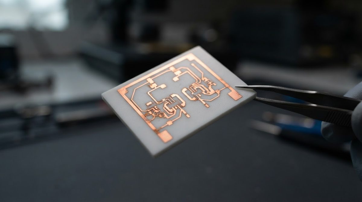
MCPCBs use an aluminum or copper base plate with a thin dielectric layer (50–150 µm) carrying the circuit. The dielectric itself conducts only 1–4 W/mK, but it is thin, so the overall thermal resistance can be acceptable for spread-out heat sources like LED arrays. Where MCPCBs fall short:
- They cannot provide electrical isolation above ~3 kV without thickening the dielectric, which kills the thermal advantage.
- The dielectric degrades above 130–150 °C, limiting use in high-temperature environments.
- CTE mismatch between the aluminum base (~23 ppm/°C) and silicon or SiC die causes reliability problems in power modules.
Ceramic substrates win on isolation voltage, operating temperature, CTE match, and raw thermal conductivity. MCPCBs win on cost and availability for large-area, moderate-power designs.
Design Choices That Complement a High-k Substrate
Even with a high thermal conductivity substrate, overall thermal resistance depends on the full stack. A few design moves make a measurable difference:
- Thermal vias. Copper-filled vias beneath a hot component create parallel heat paths through the substrate. See the thermal via design guide for fill options and pitch rules on ceramic boards.
- Copper layer thickness. Thicker copper on the back side acts as a heat spreader. DBC (direct bond copper) on AlN or Al₂O₃ typically uses 0.3 mm copper, while AMB (active metal brazing) on Si₃N₄ allows up to 0.8 mm copper.
- Solder or sintered-silver attach. The die-attach layer often dominates junction-to-case resistance. Sintered silver (k ≈ 200–250 W/mK) outperforms SAC305 solder (k ≈ 60 W/mK) by roughly 3–4×.
When NOT to Use a High Thermal Conductivity PCB
Ceramic and specialty substrates are not always the right answer. Skip them if:
- Your power density is low. A 1 W LED on a 20 mm² pad does not need AlN. Standard FR-4 with adequate copper planes, or a basic MCPCB, handles it at a fraction of the cost.
- You need large board area. Ceramic substrates are limited to roughly 150 mm × 150 mm per panel. If your design is 200 mm × 300 mm, ceramic is impractical without tiling, which adds assembly cost and thermal interfaces.
- Mechanical shock is a concern. Ceramics are brittle. A handheld consumer device that gets dropped is better served by FR-4 or a flex-rigid build.
- Budget is the primary constraint. AlN substrates can cost 40–70× the equivalent FR-4 area. If your thermal problem can be solved with a heatsink and thermal interface material on FR-4, that is the cheaper path.
Frequently Asked Questions
Is aluminum nitride always better than alumina for thermal performance?
AlN has 6–8× higher thermal conductivity than 96% alumina, so it always conducts heat faster through the substrate. However, for applications where the substrate thermal resistance is a small fraction of the total junction-to-ambient resistance, the improvement may not justify the 3–5× cost premium. Run the full Rth stack before committing to AlN.
Can I use a metal-core PCB instead of ceramic above 200 °C?
No. Standard MCPCB dielectric layers are organic and degrade above 130–150 °C. Ceramic substrates operate continuously at 300 °C or higher depending on grade and metallization. For extreme-temperature applications, ceramic is the only practical board-level option.
Does higher thermal conductivity mean lower dielectric strength?
Not for ceramics. AlN has both the highest thermal conductivity (170–200 W/mK) and a dielectric strength of 15–17 kV/mm, comparable to alumina. The two properties are independent in ceramic materials, unlike in MCPCBs where thickening the dielectric to increase isolation voltage reduces thermal performance.
What is the thinnest ceramic substrate available for maximum thermal performance?
AlN and alumina substrates are commercially available down to 0.25 mm (250 µm). Thinner substrates reduce thermal resistance proportionally, but they are more fragile and harder to handle in assembly. For most power electronics, 0.32–0.635 mm is the practical range.
How does thermal conductivity of ceramics change at high temperatures?
Thermal conductivity of AlN drops significantly with temperature—from ~180 W/mK at 25 °C to roughly 80 W/mK at 300 °C (per CoorsTek data). Alumina is more stable, dropping from ~26 W/mK to ~15 W/mK over the same range. Always use the k value at your actual operating temperature for Rth calculations, not the room-temperature spec.
For more answers to common substrate questions, explore the ceramic PCB FAQ.
Next Step
If your thermal budget points toward a ceramic substrate, the next decision is material grade and metallization process. Start with the full ceramic material comparison to narrow your options, then request a quote with your Gerber files and thermal requirements.