A ceramic PCB heat spreader works by using the substrate itself—alumina, aluminum nitride, or silicon nitride—as the primary lateral heat-spreading layer, eliminating the separate metal heat spreader found in conventional assemblies. The approach reduces interface count, lowers total thermal resistance, and shrinks the Z-height of power and LED modules. Whether it makes sense for your board depends on the die size, total dissipated power, and allowable junction temperature.
Key Takeaways
- AlN substrates (170–200 W/m·K) spread heat 6–8× more effectively than 96% alumina (24–28 W/m·K) and rival copper-clad aluminum MCPCBs in many layouts.
- Thicker copper metallization (≥ 300 µm) on a ceramic substrate adds meaningful lateral conduction, but CTE mismatch limits practical thickness—especially on AlN.
- A ceramic heat spreader eliminates one thermal interface (TIM layer between PCB and external spreader), often saving 0.3–0.8 °C/W per interface removed.
- For die dissipating more than roughly 50 W in a footprint under 10 × 10 mm, AlN or Si₃N₄ with DBC or AMB copper is the usual starting point.
- Below about 5 W total, 96% alumina with standard thick-film metallization is usually sufficient and far cheaper.
Why Ceramic Works as a Heat Spreader
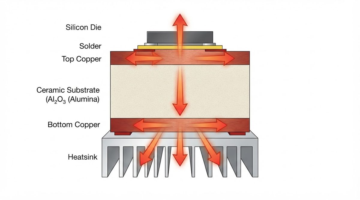
A heat spreader’s job is to take a small, high-flux heat source and distribute that energy over a larger area before it reaches the heatsink or ambient. Two substrate properties matter most: thermal conductivity of the ceramic material and the thermal expansion coefficient (CTE). Ceramic substrates sit in a useful middle ground: their thermal conductivity is lower than copper (385 W/m·K) but high enough—especially AlN—to spread heat effectively, while their CTE (4.5–7.2 ppm/°C depending on grade) closely matches silicon (2.6 ppm/°C) and SiC (4.0 ppm/°C) die. That CTE match means you can solder a bare die directly to the metallized ceramic without the cracking risk you face when soldering to a copper or aluminum spreader.
Removing the separate spreader also removes one solder or TIM joint. Each interface in a thermal stack adds 0.3–0.8 °C/W for a typical 10 × 10 mm footprint (per Infineon AN2019-09, “Thermal Resistance: Theory and Practice”). In a three-interface stack, eliminating one can cut total Rth by 15–25%.
Material Selection for Ceramic Heat Spreaders
| Parameter | Al₂O₃ 96% | Al₂O₃ 99.6% | AlN | Si₃N₄ | Unit | Condition |
|---|---|---|---|---|---|---|
| Thermal conductivity | 24–28 | 28–33 | 170–200 | 70–90 | W/m·K | 20 °C, ASTM E1461 |
| CTE | 6.5–7.2 | 6.5–7.0 | 4.5–4.8 | 2.5–3.5 | ppm/°C | 20–300 °C |
| Flexural strength | 300–350 | 350–400 | 300–350 | 650–800 | MPa | ASTM C1161 |
| Dielectric strength | ≥ 10 | ≥ 12 | ≥ 15 | ≥ 10 | kV/mm | IEC 60672 |
| Relative cost (per cm²) | 1× | 1.5× | 3–5× | 4–6× | — | Indicative, 2024 |
Typical values for commercially available material, for comparison only. Confirm against the datasheet for your specific grade.
For most ceramic heat spreader applications, the decision narrows to alumina vs. AlN. Alumina is the default for power levels under roughly 5 W per device. AlN becomes necessary when you need to keep junction temperature within spec at higher flux densities—LED COB arrays above 30 W, GaN HEMT pallets, or IGBT modules. Si₃N₄ is chosen primarily for mechanical reliability under thermal cycling (its fracture toughness is roughly 2× that of AlN), which matters in automotive power modules subject to thousands of –40 °C to +150 °C cycles. For a deeper look at maximum operating temperature limits, see the companion article.
Copper Layer as Part of the Spreader
The metallization on a ceramic substrate is not just a circuit layer—it contributes directly to lateral heat spreading. Copper’s 385 W/m·K dwarfs even AlN, so a 300 µm DBC copper layer on a 0.635 mm AlN substrate carries a meaningful share of the total lateral conduction. The combined effective thermal conductivity of the copper-ceramic-copper sandwich exceeds either material alone.
Thicker copper spreads more heat, but the CTE mismatch between copper (17 ppm/°C) and ceramic (4.5–7.2 ppm/°C) creates residual stress after the bonding process. This stress can bow the substrate or, worse, crack it during thermal cycling. DBC (direct bonded copper) processes on AlN typically top out at 300–400 µm per side. AMB (active metal brazing) can push to 800 µm or beyond on Si₃N₄ because the higher fracture toughness tolerates the stress. If your design needs thick copper on alumina, review copper plating capabilities and tolerances to confirm what is achievable for your substrate thickness.
Controlling substrate warpage and flatness is essential when the ceramic doubles as a heat spreader, because a bowed substrate creates an air gap at the heatsink interface that can add several °C/W to the thermal path.
Worked Example: AlN Heat Spreader for a 25 W GaN Die
Consider a 3 × 3 mm GaN die dissipating 25 W, soldered to a 25 × 25 mm AlN substrate (0.635 mm thick, 300 µm DBC copper both sides), which is then soldered to a copper heatsink.
Step 1: Conduction Through the Ceramic
Rth (ceramic) = t / (k × A_eff), where t = 0.635 mm, k = 180 W/m·K, and A_eff is an effective spreading area. Using a 45° spreading angle from the 3 × 3 mm source through 0.635 mm thickness, the effective area at the bottom of the ceramic ≈ (3 + 2 × 0.635)² = 4.27² ≈ 18.2 mm². Rth (ceramic) ≈ 0.000635 / (180 × 18.2 × 10⁻⁶) ≈ 0.19 °C/W.
Step 2: Copper Layers
Each 300 µm copper layer: Rth ≈ 0.0003 / (385 × 18.2 × 10⁻⁶) ≈ 0.04 °C/W. Two layers contribute about 0.08 °C/W total.
Step 3: Solder Interfaces
Die-attach solder (SAC305, ~50 W/m·K, 50 µm BLT, 9 mm² area): Rth ≈ 0.00005 / (50 × 9 × 10⁻⁶) ≈ 0.11 °C/W. Substrate-to-heatsink solder (same alloy, 100 µm BLT, 625 mm² area): Rth ≈ 0.0001 / (50 × 625 × 10⁻⁶) ≈ 0.003 °C/W.
Total and Junction Temperature
Rth (junction to heatsink) ≈ 0.11 + 0.04 + 0.19 + 0.04 + 0.003 ≈ 0.38 °C/W. ΔT = 25 W × 0.38 °C/W ≈ 9.5 °C above heatsink temperature. If the heatsink sits at 60 °C, junction temperature is about 70 °C—well within most GaN device limits.
For a more rigorous treatment including spreading resistance corrections (the 45° rule underestimates spreading resistance for small die on large substrates), see the thermal resistance calculation method article, or run a FEA model per the thermal simulation setup guide.
Layout Guidelines for Effective Heat Spreading
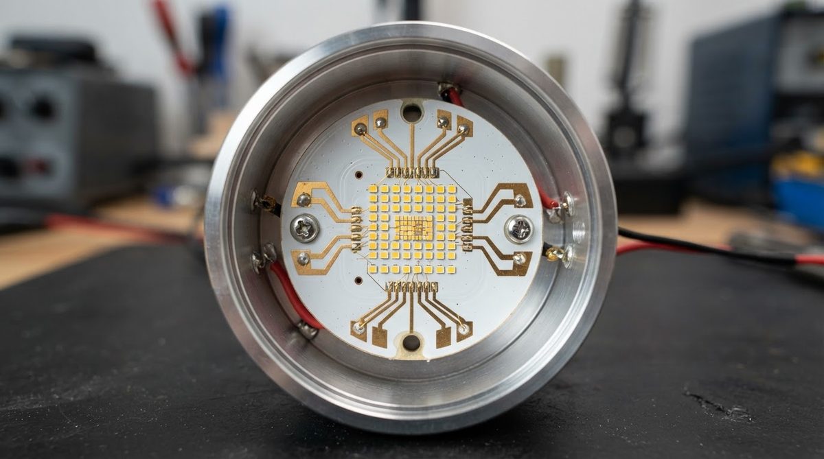
- Maximize copper pour under the die. Unbroken copper on the bottom side directly beneath the heat source provides the lowest-resistance path to the heatsink. Route traces away from this zone.
- Keep substrate thickness proportional to die size. A substrate thinner than roughly half the die edge length does not spread heat laterally before it reaches the bottom surface. For a 3 × 3 mm die, use at least 0.38 mm ceramic thickness; 0.635 mm is standard and works well.
- Symmetrize copper on both sides. Equal copper thickness top and bottom minimizes thermally induced bow. If the top side has less copper coverage, expect concave warpage after reflow.
- Place thermal vias only in alumina. AlN and Si₃N₄ substrates are dense enough that through-substrate conduction is effective without vias. On alumina, copper-filled vias can reduce Rth by 30–40%.
When NOT to Use a Ceramic Heat Spreader
A ceramic heat spreader adds cost and design constraints that are not always justified.
- Total power under 2–3 W, non-critical junction temp: FR-4 or standard MCPCB with thermal grease will meet the thermal budget at a fraction of the cost.
- Board area above ~100 × 100 mm: Large ceramic panels are expensive and fragile. A metal-core PCB or a small ceramic sub-mount bonded to an aluminum baseplate is usually more practical.
- High-vibration environments without Si₃N₄: Alumina and AlN are brittle. If the assembly sees sustained vibration or mechanical shock, and Si₃N₄ is outside the budget, a metal spreader with a compliant TIM may be more reliable.
- Designs requiring many layers: Ceramic PCBs beyond 3–4 layers are possible but costly. If you need 6+ layers of routing and heat spreading, a hybrid approach—ceramic sub-mount on a multilayer organic board—often wins.
Frequently Asked Questions
Can I use alumina instead of AlN to save cost?
Yes, if the thermal budget allows it. At 24–28 W/m·K, 96% alumina spreads heat roughly 7× less effectively than AlN. For devices under about 5 W in a 5 × 5 mm footprint, alumina is often sufficient. Run the Rth calculation with your actual die size and power before deciding.
How thick should the ceramic be for heat spreading?
A good starting point is a substrate thickness equal to 0.5–1× the die edge length. Thinner substrates do not spread laterally before heat reaches the bottom. Standard thicknesses of 0.38 mm and 0.635 mm cover most designs with die sizes from 1 × 1 mm to 5 × 5 mm.
Does a ceramic heat spreader need a separate heatsink?
Almost always, yes. The ceramic spreads heat laterally but has limited thermal mass. Without a heatsink or chassis to absorb and convect the energy, the substrate temperature will rise until it reaches a steady state that may exceed your device’s rated junction temperature.
Is DBC or AMB better for a heat spreader application?
DBC is simpler and cheaper, suitable for copper up to about 300–400 µm on AlN. AMB allows thicker copper (up to 800 µm+) and bonds more reliably to Si₃N₄, making it the preferred process for automotive-grade power modules that must survive thousands of thermal cycles per AQG 324 (ECPE guideline for automotive power modules).
Can I solder a bare die directly to the ceramic?
You solder to the metallization, not the ceramic itself. DBC and AMB copper surfaces accept standard die-attach solders (AuSn, SAC305, sintered silver). The ceramic’s low CTE means the solder joint sees less strain than it would on a copper or aluminum spreader, improving long-term reliability.
Next Step
If you have a specific die size, power level, and target junction temperature, the fastest path forward is to request a quote with your thermal requirements. Our engineers can recommend a substrate material, copper thickness, and layout approach matched to your thermal budget.