Alumina 99.6% Al2O3 custom PCBs deliver higher thermal conductivity (28–35 W/m·K at 25 °C), lower dielectric loss (tan δ ≈ 0.0001 at 1 MHz), and better hermeticity than standard 96% alumina, making them the default substrate for precision RF, high-power LED, and medical sensor circuits where 96% alumina falls short but aluminum nitride is overkill on cost. This guide covers what you need to specify when ordering a custom 99.6% alumina board.
Why 99.6% Alumina Instead of 96%?
The 3.6 percentage-point jump in purity removes most of the silica-based glass phase that binds 96% alumina. That matters in three measurable ways: thermal conductivity rises from 24–28 W/m·K to 28–35 W/m·K (per Kyocera A-493 and CoorsTek ADS-996 datasheets, measured at 25 °C per ASTM E1461); dielectric loss drops roughly by half; and surface finish improves to Ra ≤ 0.3 µm as-fired, which tightens thin-film line definition. For a full property comparison, see the 99.6% alumina material properties datasheet.
The trade-off is cost. High-purity powder is more expensive, sintering temperatures are higher (1 600–1 700 °C vs. 1 500–1 600 °C for 96%), and the harder surface wears tooling faster during laser scribing and drilling. Expect to pay 1.5–2.5× the unit price of an equivalent 96% alumina custom PCB at comparable volumes.
Metallisation Processes for 99.6% Al2O3 Custom Boards
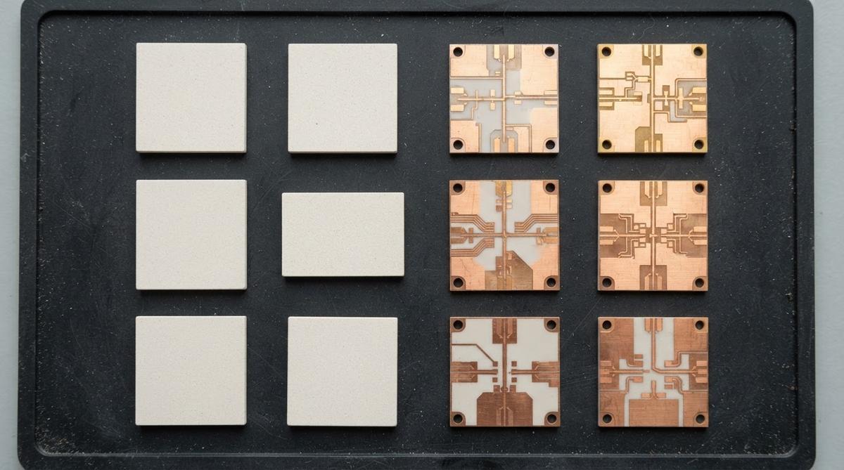
Three metallisation routes dominate custom 99.6% alumina work. The right choice depends on your line width, current capacity, and budget.
| Process | Typical Cu thickness | Min trace / space | Best for |
|---|---|---|---|
| DPC (Direct Plated Copper) | 1–10 µm | 20–30 µm / 20–30 µm | Fine-line RF, sensors, thin-film hybrids |
| Thick film (screen print) | 10–25 µm (Ag, Au, AgPd) | 100–150 µm / 100–150 µm | Wire-bond pads, resistor networks, cost-sensitive runs |
| DBC (Direct Bonded Copper) | 127–635 µm (5–25 mil) | 200–300 µm / 200–300 µm | High-current power modules, LED thermal paths |
Typical values for commercially available processes, for comparison only. Confirm against the datasheet for your specific grade.
DPC on 99.6% alumina is the sweet spot for most precision applications. The low surface roughness of high-purity alumina improves sputtered seed-layer adhesion, which in turn yields tighter line definition than the same process on 96% substrates. If your design requires copper thicker than about 100 µm for current handling, DBC is the practical route, though minimum feature sizes widen considerably.
Key Specifications to Define Before Ordering
A complete custom 99.6% alumina PCB order needs these parameters locked down. Missing any of them adds a design-review cycle and delays your prototype.
- Substrate dimensions and thickness. Common thicknesses range from 0.25 mm to 2.0 mm. Thinner substrates (≤ 0.38 mm) require careful handling fixtures; specify whether you need them panelised or singulated.
- Metallisation type and layer count. Single-sided, double-sided, or multi-layer. For double-sided DPC, specify via method (laser-drilled and plated, or through-substrate via paste).
- Copper thickness and surface finish. ENIG, ENEPIG, immersion silver, and bare gold are typical. The finish affects wire-bondability, solderability, and shelf life.
- Dimensional and positional tolerances. Standard laser-cut tolerance on fired 99.6% alumina is ±0.05 mm; tighter tolerances (±0.025 mm) require post-fire grinding, adding cost.
- Quantity and panel format. Prototypes (1–25 pcs) often run on shared panels. Production runs benefit from dedicated tooling.
Worked Example: Thermal Resistance of a 99.6% Alumina Substrate
Suppose you are mounting a 3 W UV LED die on a 10 mm × 10 mm × 0.635 mm thick 99.6% alumina substrate. The one-dimensional thermal resistance through the ceramic alone is:
Rth = t / (k × A)
where t = 0.635 × 10⁻³ m, k = 30 W/m·K (mid-range for 99.6% Al2O3), A = 1 × 10⁻⁴ m².
Rth = 0.000635 / (30 × 0.0001) = 0.21 °C/W
At 3 W dissipation, the temperature drop across the ceramic is 0.63 °C. Compare this with 96% alumina at 25 W/m·K: Rth = 0.25 °C/W, ΔT = 0.76 °C. The difference is small for a single LED. Where 99.6% alumina earns its premium is in dense arrays or high-frequency circuits where the lower dielectric loss matters more than the modest thermal gain. For applications needing a larger thermal jump, consider custom aluminum nitride (AlN) fabrication, which offers 170–200 W/m·K.
CTE Matching Considerations
99.6% alumina has a CTE of approximately 7.1–7.4 ppm/°C (20–400 °C, per CoorsTek ADS-996). This is close to GaAs (5.7 ppm/°C) and SiC (4.0 ppm/°C) but a poor match to copper (17 ppm/°C). In power-cycling applications, the CTE mismatch between thick copper layers and the substrate drives crack initiation at the bond interface. Design rules to manage this include limiting copper thickness, adding stress-relief patterns, and selecting solder alloys with some compliance. A deeper discussion is on the CTE matching in ceramic PCB design page.
When NOT to Use 99.6% Alumina
Cost-driven consumer products. If your thermal and dielectric requirements are met by 96% alumina, the higher cost of 99.6% adds no value. Run the numbers on both grades before committing.
Extreme thermal loads (>50 W/cm²). At very high flux densities, even 35 W/m·K is insufficient. AlN (170–200 W/m·K) or custom silicon nitride substrates (for mechanical toughness under thermal cycling) are better choices.
Large-area boards (>150 mm × 150 mm). Ceramic substrates are brittle. Boards larger than about 150 mm on a side need careful mechanical support or should be segmented into sub-modules on a metal baseplate.
Standard digital logic. FR-4 or metal-core PCBs handle most digital circuits at a fraction of the cost. Ceramic is warranted only when thermal, dielectric, or hermeticity requirements exceed what organic laminates can deliver.
Frequently Asked Questions
What is the maximum operating temperature for a 99.6% alumina PCB?
The ceramic substrate itself withstands continuous use above 1 000 °C. The practical limit is set by the metallisation and solder: thick-film gold circuits can operate to roughly 500 °C, while standard SAC305 solder joints limit assemblies to about 150 °C. High-temperature solders (AuSn, AuGe) push that to 280–350 °C.
Can I get double-sided vias on 99.6% alumina?
Yes. Laser-drilled vias filled with plated copper (DPC process) or conductive via paste (thick-film process) are standard. Minimum via diameters are typically 0.1–0.15 mm for laser-drilled holes in 0.25–0.635 mm substrates.
How does 99.6% alumina compare to AlN on cost?
99.6% alumina costs roughly 30–50% of equivalent AlN substrates per unit area, depending on size and volume. AlN is justified only when the thermal conductivity of alumina is genuinely insufficient for your power density.
What file formats do I need for a custom order?
Gerber RS-274X is standard for circuit layers. Include an Excellon drill file for vias and a DXF or STEP file for the substrate outline. A fabrication drawing (PDF) specifying tolerances, finishes, and stack-up completes the package.
Is 99.6% alumina suitable for wire bonding?
Yes. The smooth as-fired surface (Ra ≤ 0.3 µm) and high-purity metallisation pads make 99.6% alumina an excellent wire-bond substrate. Gold wire bonding to thick-film gold pads and aluminium wedge bonding to DPC pads are both proven processes.
Next Step
If your design calls for high-purity alumina, start by reviewing the 99.6% alumina PCB sourcing and properties overview to confirm the grade fits your electrical and thermal requirements. Then submit your Gerber files and substrate specs for a quote.