Ceramic PCB CTE matching means selecting a substrate whose coefficient of thermal expansion is close enough to the bonded die, solder, or copper layer that thermomechanical stress stays below the fatigue limit over the product’s lifetime. Get the match wrong and you get cracked solder joints, delaminated die attach, or substrate fracture, often within a few hundred thermal cycles. Proper ceramic PCB CTE matching is the single highest-leverage reliability decision in any bare-die or power-module assembly.
Key Takeaways
- Silicon has a CTE of roughly 2.6 ppm/°C at 25 °C; aluminum nitride (AlN) at 4.5–5.0 ppm/°C is the closest common ceramic match.
- 96% alumina (Al₂O₃) at 6.5–7.2 ppm/°C is acceptable for many power packages but produces roughly 2× the mismatch stress versus AlN when bonding bare silicon die.
- Silicon nitride (Si₃N₄) at 2.5–3.5 ppm/°C offers the tightest CTE match to silicon and is chosen mainly for its fracture toughness in high-cycle environments.
- Underfill or compliant die-attach materials can compensate for 2–3 ppm/°C of mismatch, but they add process steps and cost.
- CTE mismatch stress scales linearly with ΔT and ΔCTE—halving the temperature swing or halving the CTE gap each cut stress by half.
What Is CTE and Why Does Ceramic PCB CTE Matching Matter?
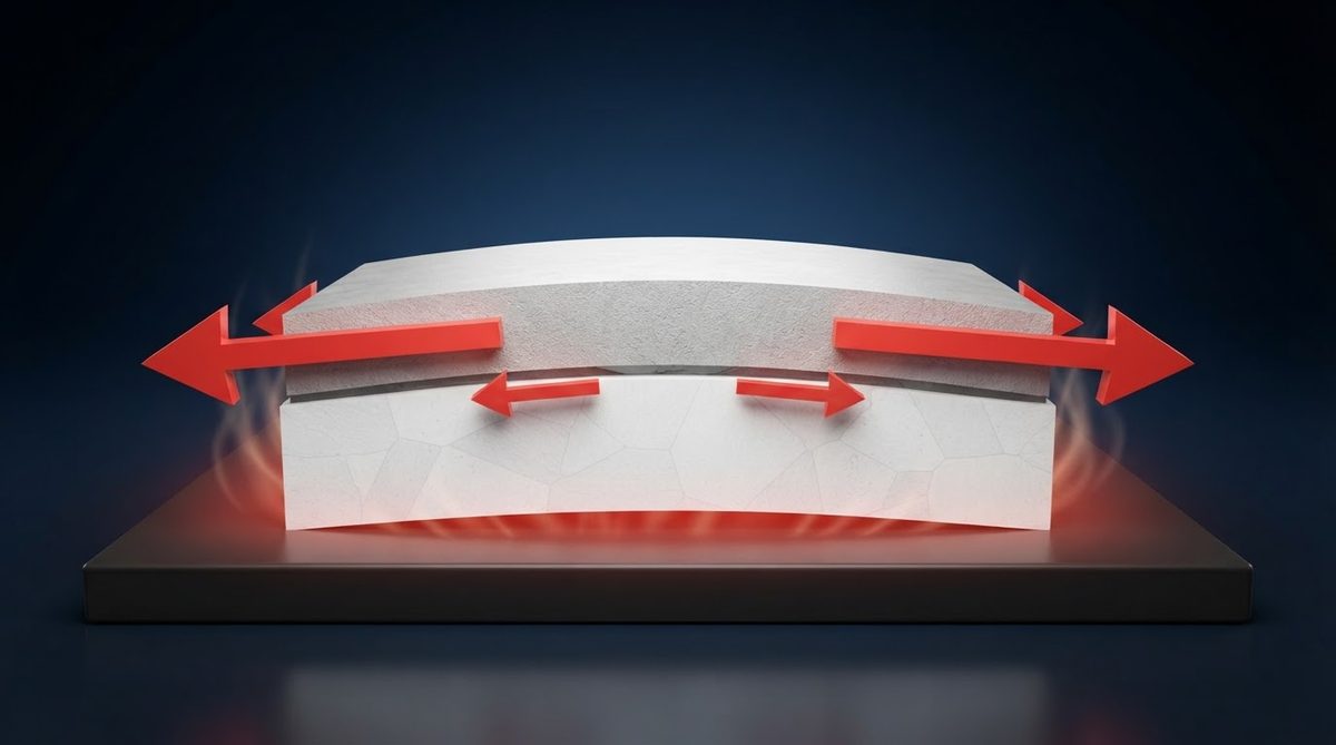
CTE (coefficient of thermal expansion) describes how much a material expands per degree of temperature change, expressed in ppm/°C (parts per million per degree Celsius). Every material in a PCB assembly—substrate, copper trace, solder, die—has its own CTE. When the assembly heats up during operation or reflow, each layer tries to expand by a different amount. The difference creates shear stress at every bonded interface.
Ceramic substrates are inherently better matched to semiconductor die than organic laminates. FR-4 has a CTE of 14–17 ppm/°C in-plane, which is 5–6× that of silicon. Alumina at 6.5–7.2 ppm/°C cuts that gap by more than half. AlN at 4.5–5.0 ppm/°C cuts it further. This advantage in ceramic PCB CTE matching is one of the core reasons power electronics, RF modules, and LED packages use ceramic substrates at all.
The stress is not just about peak temperature. It accumulates with every thermal cycle—power-on to power-off, ambient swing, reflow. Solder-joint fatigue life follows Coffin-Manson relationships: doubling the cyclic shear strain can reduce life by 4–8×. Selecting the right substrate CTE is the single highest-leverage decision you make to extend reliability.
CTE Values for Common Substrate and Die Materials
| Material | CTE (ppm/°C) | Condition | Source |
|---|---|---|---|
| Silicon (Si) | 2.6 | 25 °C | SEMI M1-0302 |
| Silicon carbide (SiC) | 4.0–4.5 | 25–400 °C | Wolfspeed datasheet |
| Gallium nitride on Si | 2.6 (substrate-dominated) | 25 °C | Cree/Wolfspeed app note |
| Gallium arsenide (GaAs) | 5.7–6.0 | 25–200 °C | AXT Inc. datasheet |
| Aluminum nitride (AlN) | 4.5–5.0 | 25–400 °C, per ASTM E228 | Kyocera SH-30 datasheet |
| Silicon nitride (Si₃N₄) | 2.5–3.5 | 25–400 °C | Kyocera SN series datasheet |
| Al₂O₃ 96% | 6.5–7.2 | 25–400 °C, per ASTM E228 | CoorsTek ADS-96R datasheet |
| Al₂O₃ 99.6% | 7.1–8.0 | 25–400 °C | CoorsTek ADS-996 datasheet |
| Copper (Cu) | 16.5–17.0 | 25 °C | ASM Handbook Vol. 2 |
| SAC305 solder | 21–23 | 25 °C | IPC-SM-785 |
| FR-4 (in-plane) | 14–17 | 25–260 °C | IPC-4101E |
Typical values for commercially available material, for comparison only. Confirm against the datasheet for your specific grade.
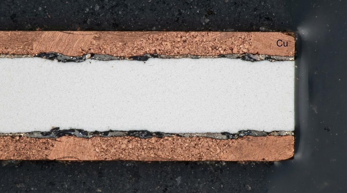
Notice the copper layer itself is a mismatch source. On a DBC (direct bond copper) substrate, the 0.3 mm copper at 17 ppm/°C bonded to AlN at 4.5 ppm/°C creates bowing and edge stress. Symmetric copper on both sides is standard practice to balance this stress. If your design requires copper on one side only, expect warpage on the order of 50–150 µm across a 50 × 50 mm tile after brazing, depending on copper thickness.
Worked Example: Estimating Die-Attach Shear Stress from CTE Mismatch
A simplified elastic model gives a first-order estimate of the shear stress at a bonded interface. This is not a substitute for FEA, but it tells you whether your ceramic PCB CTE matching is in the right ballpark before you commit to a substrate.
Setup: A 5 × 5 mm bare silicon die is soldered (SAC305, 50 µm bond line) to a 96% alumina substrate. The assembly cycles from 25 °C to 150 °C (ΔT = 125 K).
- CTE mismatch (ΔCTE): 7.0 − 2.6 = 4.4 ppm/°C
- Free thermal strain: ΔCTE × ΔT = 4.4 × 10⁻⁶ × 125 = 5.5 × 10⁻⁴
- Maximum differential displacement at the die corner (half-diagonal = 3.54 mm): δ = 5.5 × 10⁻⁴ × 3.54 mm = 1.95 µm
- Shear strain in solder: γ = δ / bond-line thickness = 1.95 / 50 = 0.039 (3.9%)
- Estimated shear stress (using SAC305 elastic shear modulus ~19 GPa at 25 °C, acknowledging creep will relax this): τ ≈ G × γ = 19,000 × 0.039 = 741 MPa (elastic peak; real creep-relaxed stress is much lower, typically 20–40 MPa at steady state)
Now repeat with AlN (CTE 4.7 ppm/°C): ΔCTE = 2.1 ppm/°C, displacement = 0.93 µm, shear strain = 1.9%. The strain is halved, and because Coffin-Manson fatigue life scales as strain to the power of −1.9 to −2.5, that halved strain roughly quadruples solder-joint life. This is why AlN is the default for bare-die power modules cycling above ΔT = 100 K.
Enter your own die size, substrate material, and temperature range to estimate interface stress and see whether your ceramic PCB CTE matching is adequate for your target cycle life.
[pcb_calc type=”ceramic-substrate-match”]
How to Choose the Right Substrate for Ceramic PCB CTE Matching
The decision depends on three variables: the die material, the operating temperature swing, and the required cycle life.
Silicon or GaN-on-Si die, ΔT > 100 K, > 3 000 cycles: AlN is the standard choice. Its CTE of 4.5–5.0 ppm/°C keeps mismatch under 2.5 ppm/°C versus silicon. Its thermal conductivity of 170–200 W/mK also helps limit ΔT in the first place. For extreme cycle counts (> 15 000 cycles, automotive AEC-Q101), silicon nitride material properties make Si₃N₄ attractive: CTE 2.5–3.5 ppm/°C (near-perfect silicon match) and fracture toughness of 6–7 MPa·√m, roughly 3× that of AlN.
SiC die, ΔT 80–150 K: SiC at 4.0–4.5 ppm/°C matches AlN almost exactly. This fortunate coincidence has made AlN + DBC the dominant platform for SiC MOSFET power modules (Infineon, Wolfspeed). Al₂O₃ adds roughly 2.5 ppm/°C of mismatch and is generally acceptable only for lower cycle-count applications or with compliant attach.
GaAs die (RF, MMIC): GaAs at 5.7–6.0 ppm/°C is surprisingly close to 96% alumina. For RF applications below 150 °C junction temperature with moderate cycle counts, alumina is often the most cost-effective substrate. Use a ceramic substrate selection guide to weigh CTE, dielectric constant, and cost together.
Mitigating CTE Mismatch When You Cannot Change the Substrate
Sometimes the substrate is locked by thermal conductivity, dielectric, or cost requirements, and the CTE gap is larger than ideal. Several techniques reduce the effective stress without changing the ceramic material:
- Underfill: Distributes shear strain across the entire bond area instead of concentrating it at solder-joint edges. Adds a process step and complicates rework.
- Compliant die-attach (silver sintering, soft solders): A thicker, more compliant bond line absorbs more strain. Silver-sintered joints are increasingly common in automotive SiC modules.
- Smaller die or tiled die: Mismatch displacement scales with die diagonal. Two 3 × 3 mm die produce less corner stress than one 5 × 5 mm die on the same substrate.
- Symmetric metallisation: Copper on both sides of the substrate balances bowing stress. This is standard for DBC and AMB substrates.
- Stress-relief patterning: Dimples or slots in the copper near the die edge reduce local constraint. Common in ceramic heat spreader designs for high-power modules.
When CTE Matching Is Not Your Priority
If your assembly uses only surface-mount passives and packaged ICs (QFN, BGA with organic interposer), the package itself absorbs most CTE mismatch. A 96% alumina substrate at 7 ppm/°C works fine with standard SAC305 solder and no underfill for most commercial and industrial temperature ranges (−40 to +85 °C). Spending extra on AlN purely for CTE reasons is unnecessary in this case.
Similarly, if your board operates at near-constant temperature (e.g., a sensor in a controlled oven), thermal cycling is minimal and CTE mismatch rarely causes failures. Prioritise ceramic dielectric performance or cost instead.
For applications with no bare die, low cycle counts, and junction temperatures under 100 °C, FR-4 or metal-core PCBs may be entirely adequate—and far cheaper.
Frequently Asked Questions
Does CTE mismatch cause problems during reflow or only in operation?
Both. Reflow subjects the assembly to ΔT of 200+ K in minutes. A large CTE mismatch can crack brittle ceramic substrates or fracture solder joints during cooldown from peak reflow temperature. Operational cycling then accumulates fatigue damage over time.
Can I use alumina instead of AlN for bare silicon die?
Yes, if the temperature swing is moderate (ΔT < 80 K) and the required cycle life is under roughly 2 000 power cycles. Above that, the 4.4 ppm/°C mismatch between 96% alumina and silicon typically drives solder-joint failures. Underfill or compliant attach can extend life, but AlN is the more reliable long-term choice for ceramic PCB CTE matching with silicon.
What CTE does copper add to a ceramic substrate stack?
Copper itself does not change the substrate’s CTE, but the composite CTE of a DBC assembly shifts toward copper’s 17 ppm/°C as copper thickness increases relative to ceramic thickness. A 0.3 mm Cu / 0.63 mm AlN / 0.3 mm Cu stack has an effective in-plane CTE of roughly 7–8 ppm/°C, per CeramTec curamik application notes.
Is silver sintering better than solder for CTE-mismatched joints?
Silver-sintered die attach has higher thermal conductivity (~200 W/mK vs ~60 W/mK for SAC305) and better fatigue resistance under thermal cycling. It tolerates larger CTE mismatches than solder for the same cycle life. The trade-off is higher process temperature (typically 250–300 °C with pressure) and higher material cost.
How do I measure CTE mismatch effects in my prototype?
The standard method is thermal cycling per JEDEC JESD22-A104 (e.g., −40 to +150 °C, 1 000 cycles) followed by cross-sectioning and C-SAM (acoustic microscopy) to detect delamination or solder cracks. Warpage can be measured during cycling with shadow moiré or digital image correlation (DIC).
Next Step
If you are selecting a substrate for a bare-die or high-reliability assembly, start with the CTE table above and the calculator to narrow your material choice. For detailed Si₃N₄ substrate datasheets or AlN specifications, request them directly. When you are ready to quote a specific design, check the ceramic PCB FAQ for file-prep details or submit your files for a quote.