An alumina 99.6% Al2O3 PCB is a ceramic circuit board made from alumina with a purity of 99.6%, offering thermal conductivity of 28–35 W/mK at 25 °C, dielectric strength above 15 kV/mm, and a usable temperature ceiling exceeding 1 700 °C. It sits between the workhorse 96% alumina grade and costlier aluminum nitride, filling a performance gap that matters in high-frequency, high-power, and precision-sensor designs. Engineers evaluating an alumina 99.6% Al2O3 PCB for a new project should weigh the tighter dielectric tolerance and improved thermal path against the 1.5–2.5× cost premium over 96% alumina.
Key takeaways:
- 99.6% alumina conducts heat 15–25% better than 96% alumina (28–35 W/mK vs. 24–28 W/mK at 25 °C, per Kyocera A-493 and CoorsTek ADS-996 datasheets).
- Dielectric constant is 9.7–9.9 at 1 MHz, tighter than the 9.0–9.5 range of 96% grades, which simplifies RF impedance matching.
- Flexural strength reaches 350–400 MPa (ASTM C1161, 4-point bend), roughly 20% above 96% alumina.
- Cost per unit area runs 1.5–2.5× that of 96% alumina, depending on substrate size and metallization process.
- Standard metallization routes include thick film, thin film (sputtered), and DPC; DBC is used less often due to the higher sintering temperatures required for 99.6% bodies.
What Makes an Alumina 99.6% Al2O3 PCB Different from a 96% Board?
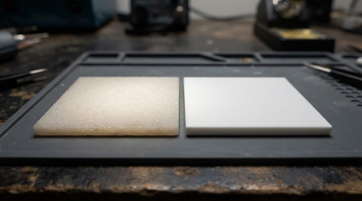
The 3.6-percentage-point purity gap is not trivial. In a 96% alumina body, the remaining 4% is a glassy silicate phase added to lower the sintering temperature. That glass phase limits thermal conductivity, softens the grain boundaries, and introduces dielectric loss at microwave frequencies. Removing most of it in a 99.6% body yields a denser, more crystalline microstructure. Grain size drops below 2 µm in fine-grained 99.6% grades, which tightens surface finish after lapping and improves thin-film adhesion.
For circuit designers, the practical differences show up in three places. First, the tighter dielectric constant tolerance (±0.1 vs. ±0.3 for 96%) means less unit-to-unit impedance variation on RF lines. Second, the lower loss tangent (0.0001–0.0003 at 1 MHz vs. 0.0002–0.0010 for 96%) reduces signal attenuation in millimeter-wave circuits. Third, the higher flexural strength makes thinner substrates viable; a 0.25 mm sheet of 99.6% alumina survives handling and assembly stresses that would crack a 96% sheet of the same thickness. For a detailed comparison of the 96% grade, see 96% alumina ceramic PCB properties.
Material Properties Table: 99.6% Al2O3
| Parameter | Value | Unit | Condition | Source |
|---|---|---|---|---|
| Purity | 99.6 | % | — | CoorsTek ADS-996 |
| Density | 3.89–3.96 | g/cm³ | Archimedes method | Kyocera A-493 |
| Thermal conductivity | 28–35 | W/mK | 25 °C, ASTM E1461 | CoorsTek ADS-996 / Kyocera A-493 |
| CTE | 7.9–8.2 | ppm/°C | 25–400 °C | Kyocera A-493 |
| Dielectric constant (εr) | 9.7–9.9 | — | 1 MHz, 25 °C | CoorsTek ADS-996 |
| Loss tangent (tan δ) | 0.0001–0.0003 | — | 1 MHz, 25 °C | Kyocera A-493 |
| Dielectric strength | 15–20 | kV/mm | DC, 25 °C, ASTM D149 | CoorsTek ADS-996 |
| Flexural strength | 350–400 | MPa | 4-pt bend, ASTM C1161 | CoorsTek ADS-996 |
| Volume resistivity | >10¹⁴ | Ω·cm | 25 °C | Kyocera A-493 |
| Max use temperature | 1 700+ | °C | In inert atmosphere | CeramTec Rubalit 710 |
| Surface roughness (as-fired) | 0.3–0.6 | µm Ra | — | Kyocera A-493 |
Typical values for commercially available material, for comparison only. Confirm against the datasheet for your specific grade.
For the full datasheet with temperature-dependent curves, see the 99.6% alumina material properties page.
Worked Example: Thermal Resistance of an Alumina 99.6% Al2O3 PCB Submount
Suppose you need to mount a 10 W laser diode on a 99.6% alumina submount measuring 10 mm × 10 mm × 0.5 mm. Thermal resistance through the substrate (one-dimensional approximation):
Rth = t / (k × A)
Where t = 0.5 mm = 0.0005 m, k = 30 W/mK (mid-range for 99.6% alumina), A = 10 × 10 mm = 0.0001 m².
Rth = 0.0005 / (30 × 0.0001) = 0.167 °C/W
At 10 W dissipation, the temperature drop across the substrate is 1.67 °C. If you ran the same calculation with 96% alumina at 25 W/mK, Rth rises to 0.200 °C/W and ΔT to 2.0 °C. The 0.33 °C difference seems small, but in a multi-die array with stacked thermal resistances, it compounds. If you need the ΔT below 0.5 °C in this footprint, you would step up to aluminum nitride substrates at 170–200 W/mK.
Enter your own substrate dimensions, thickness, and dissipated power below to estimate junction temperature rise for any alumina 99.6% Al2O3 PCB layout:
Where Alumina 99.6% Al2O3 PCBs Are Used
RF and Microwave Circuits
Millimeter-wave filters, couplers, and antenna feed networks benefit from the tight εr tolerance and low tan δ. At 10 GHz, the loss tangent of 99.6% alumina stays below 0.0004 (per Kyocera A-493 datasheet), which keeps insertion loss manageable on stripline and microstrip topologies. The stable dielectric constant also means that production units track the prototype impedance closely, reducing RF tuning time.
High-Power LED and Laser Submounts
UV-C LEDs and edge-emitting laser diodes generate intense heat flux in small footprints. An alumina 99.6% Al2O3 PCB submount with thin-film metallization (Ti/Pt/Au or TiW/Au) provides the combination of flatness (< 0.1 µm Ra after lapping), solderability, and thermal path that these devices require. For substrates below 0.38 mm, see 99.6% alumina thin substrates.
High-Temperature Sensors and Downhole Electronics
Oil-well logging tools, exhaust-gas sensors, and turbine-blade monitoring circuits operate at 300–600 °C. At these temperatures, FR-4 and polyimide flex are long gone. A 99.6% alumina substrate maintains its mechanical and dielectric properties with negligible degradation up to at least 1 000 °C, far beyond what the attached components can tolerate.
Medical Implant Electronics
Hermetic packages for pacemakers and cochlear implants often use 99.6% or higher purity alumina because the glassy phase in 96% alumina can leach trace alkali ions in body fluids. The higher purity reduces this risk and meets biocompatibility requirements under ISO 10993.
99.6% Alumina vs. Alternative Ceramic Substrates
| Parameter | 99.6% Al2O3 | 96% Al2O3 | AlN | Si3N4 |
|---|---|---|---|---|
| Thermal conductivity (W/mK, 25 °C) | 28–35 | 24–28 | 170–200 | 70–90 |
| CTE (ppm/°C, 25–400 °C) | 7.9–8.2 | 7.2–8.0 | 4.3–4.7 | 2.5–3.5 |
| Dielectric constant (1 MHz) | 9.7–9.9 | 9.0–9.5 | 8.5–8.9 | 8.0–8.5 |
| Flexural strength (MPa) | 350–400 | 280–340 | 300–350 | 700–900 |
| Fracture toughness (MPa·√m) | 3.5–4.0 | 3.0–3.5 | 2.5–3.0 | 6–7 |
| Relative cost (96% Al2O3 = 1×) | 1.5–2.5× | 1× | 3–5× | 5–8× |
Typical values for commercially available material, for comparison only. Confirm against the datasheet for your specific grade. Sources: CoorsTek, Kyocera, Maruwa datasheets.
If your thermal budget demands more than 35 W/mK, an alumina 99.6% Al2O3 PCB will not close the gap; step up to AlN. If mechanical shock and vibration are the dominant concern, silicon nitride PCBs offer roughly double the fracture toughness. For applications that need both high thermal conductivity and extreme toughness (e.g., EV power modules under thermal cycling), Si3N4 with AMB metallization is the current industry direction.
Metallization Options for 99.6% Alumina
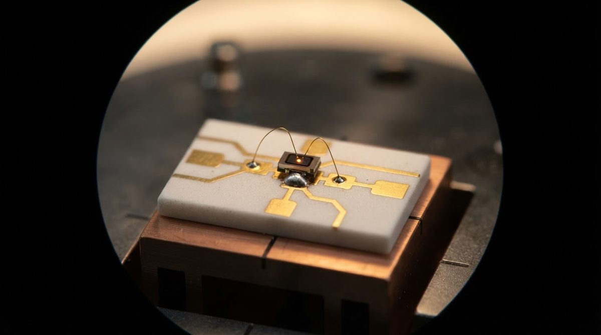
The choice of metallization depends on line resolution, adhesion requirements, and operating temperature.
Thick film (screen-printed): Ag, Au, or Ag/Pd pastes fired at 850–950 °C. Line/space down to about 100 µm. Lowest cost per board. Good for hybrid circuits and sensor pads.
Thin film (sputtered/evaporated): Ti/Pt/Au, TiW/Au, or Cr/Ni/Au stacks. Line/space below 25 µm. Excellent adhesion on lapped 99.6% surfaces due to the fine grain structure. Preferred for RF circuits and laser submounts.
DPC (Direct Plated Copper): Sputtered seed layer followed by electrolytic Cu plating. Copper thickness up to 50–100 µm. Combines fine-line capability with high current capacity. Well suited for power LED boards and high-density interconnects.
DBC (Direct Bonded Copper): Possible on 99.6% alumina, but the higher sintering temperature of the body can narrow the Cu-O eutectic bonding window. Many fabricators prefer DBC on 96% alumina or AlN and reserve 99.6% alumina for thin-film or DPC routes.
Sourcing and Cost Considerations
99.6% alumina substrates cost more than 96% primarily because the raw powder is purer and the sintering temperature is higher (1 600–1 700 °C vs. 1 500–1 600 °C for 96%), increasing furnace energy and reducing throughput. Expect to pay 1.5–2.5× the unit price of an equivalent 96% alumina board.
Lead times depend on whether you need bare substrates or metallized boards. Bare 99.6% alumina substrates in standard sizes (e.g., 50.8 × 50.8 mm, 114.3 × 114.3 mm) are often stocked by substrate manufacturers. Custom-metallized boards typically require 3–5 weeks for prototypes. For volume orders, see 99.6% alumina wholesale pricing and lead times.
When requesting quotes for an alumina 99.6% Al2O3 PCB, specify: purity grade (99.6%, not just “high-purity alumina”), substrate dimensions and thickness tolerance, surface finish (as-fired vs. lapped/polished with target Ra), metallization type and layer count, and any CTE matching requirements for die attach.
When Not to Use 99.6% Alumina
Standard digital or analog boards below 1 GHz: 96% alumina or even FR-4 will work at a fraction of the cost. The tighter εr tolerance of a 99.6% grade adds no value at these frequencies.
Thermal loads above 50 W/cm²: At high heat flux densities, the 28–35 W/mK conductivity of 99.6% alumina is insufficient. AlN at 170–200 W/mK is the correct choice, despite the higher price.
Large-panel power modules under deep thermal cycling: The CTE mismatch between alumina (7.9–8.2 ppm/°C) and silicon (2.6 ppm/°C) or SiC (4.0 ppm/°C) causes solder-joint fatigue. Si3N4 with AMB copper offers both better CTE compatibility with SiC and far higher fracture toughness.
Cost-sensitive consumer electronics: If the BOM target is under $0.50 per substrate, an alumina 99.6% Al2O3 PCB is not realistic. Metal-core PCBs (MCPCBs) or 96% alumina are more appropriate.
Frequently Asked Questions
Can I solder directly to a 99.6% alumina PCB?
Yes, provided the surface is metallized. Bare alumina is not solderable. Thick-film Au or Ag pads accept standard Sn-Ag-Cu (SAC) solder, and thin-film Ni/Au finishes are compatible with Au-Sn eutectic solder used in hermetic and optoelectronic packaging. Always verify pad adhesion strength (pull test per MIL-STD-883, Method 2011) before committing to production.
Is 99.6% alumina safe to machine or laser-cut?
Alumina dust is classified as a nuisance particulate, not a carcinogen. Standard dust extraction and PPE (N95 or better) are sufficient for machining and scribing operations. This contrasts sharply with beryllium oxide, whose dust is a confirmed carcinogen requiring specialized controls.
What surface roughness can I get on a 99.6% alumina substrate?
As-fired surfaces typically measure 0.3–0.6 µm Ra. Lapping brings this to 0.05–0.15 µm Ra, and polishing can achieve below 0.02 µm Ra. Thin-film metallization generally requires a lapped surface (Ra < 0.1 µm) for reliable adhesion and line definition.
Does 99.6% alumina outperform AlN at any frequency?
At frequencies below about 20 GHz, 99.6% alumina’s loss tangent is comparable to AlN’s, and its higher εr allows physically smaller resonators and matching networks. Above 20 GHz, AlN’s lower εr (8.5–8.9) and lower loss tangent give it an edge. The choice depends on your frequency band and thermal load, not a blanket material ranking. For detailed AlN dielectric data, see AlN dielectric properties for PCB design.
What is the minimum substrate thickness available in 99.6% alumina?
Standard catalogs list substrates as thin as 0.127 mm (5 mil). Thinner sheets (down to 0.1 mm) are available on a custom basis but require careful handling fixtures during metallization and assembly. Thinner substrates reduce thermal resistance but increase fragility.
How does 99.6% alumina compare to zirconia-toughened alumina (ZTA)?
ZTA adds 10–20% zirconia to an alumina matrix, boosting fracture toughness to 5–8 MPa·√m while slightly reducing thermal conductivity to 20–28 W/mK. If your primary concern is mechanical robustness rather than thermal or dielectric performance, ZTA ceramic PCBs may be the better fit.