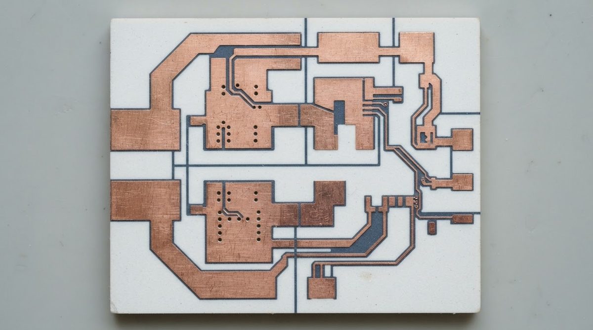
Aluminum nitride AlN custom ceramic PCBs offer thermal conductivity of 170–200 W/mK at 25 °C, roughly 6–8× higher than 96% alumina, making them the substrate of choice when heat extraction from a die or component is the primary design constraint. Custom fabrication lets you match substrate dimensions, metallization patterns, and surface finishes to a specific power module, laser diode, or RF package rather than working around catalog sizes. If your project demands precise thermal management on a non-standard footprint, an aluminum nitride AlN custom board is where the engineering starts.
Key Takeaways
- AlN thermal conductivity ranges from 170 to 200 W/mK at 25 °C depending on grain size and sintering purity (per Kyocera SH-170 and Maruwa AN-200 datasheets).
- Its coefficient of thermal expansion (CTE) of 4.5–4.7 ppm/°C closely matches silicon (2.6 ppm/°C) and SiC (4.0 ppm/°C), reducing solder-joint fatigue in die-attach applications.
- Common metallization routes for aluminum nitride AlN custom boards include DBC (direct bond copper), DPC (direct plated copper), and thin-film sputtering—each with different minimum trace widths and copper thickness limits.
- AlN is more expensive and more moisture-sensitive than alumina; specify it only when thermal resistance or CTE match justifies the cost premium.
Aluminum Nitride AlN Custom Substrate Properties at a Glance
| Parameter | Value | Unit | Condition | Source |
|---|---|---|---|---|
| Thermal conductivity | 170–200 | W/mK | 25 °C | Kyocera SH-170 / Maruwa AN-200 datasheets |
| CTE | 4.5–4.7 | ppm/°C | 20–400 °C | CoorsTek ADS-996 datasheet |
| Dielectric constant (εr) | 8.5–8.9 | — | 1 MHz, 25 °C | Maruwa AN-200 datasheet |
| Dielectric strength | 14–17 | kV/mm | 25 °C | CoorsTek ADS-996 datasheet |
| Flexural strength | 300–400 | MPa | ASTM C1161, 3-pt bend | Kyocera SH-170 datasheet |
| Volume resistivity | >10¹⁴ | Ω·cm | 25 °C | Maruwa AN-200 datasheet |
| Max continuous use temp. | ~1 000 | °C | In inert / N₂ atmosphere | CeramTec technical note |
Typical values for commercially available material, for comparison only. Confirm against the datasheet for your specific grade.
For a deeper comparison of different purity levels and how they affect thermal performance, see AlN grades and purity levels compared.
Metallization Options for Aluminum Nitride AlN Custom Boards
The metallization method determines your minimum feature size, copper thickness, and bonding strength. Three processes dominate aluminum nitride AlN custom fabrication work:
DPC (Direct Plated Copper)
A sputtered Ti/Cu seed layer followed by electroplating. Achieves line/space down to 50 µm on production panels, with copper thickness typically 1–5 oz (35–175 µm). DPC is the go-to for fine-pitch patterns on power LED carriers and laser submounts.
DBC (Direct Bond Copper)
Copper foil bonded to AlN through a controlled-atmosphere oxidation process at ~1 065 °C. Typical copper thickness is 0.3 mm (8.5 oz), suitable for high-current power modules. Minimum trace width is wider than DPC—usually ≥ 0.3 mm—because the copper is etched from a solid sheet.
Thin-Film Sputtering
Ti/Pt/Au or Ti/Ni/Au stacks sputtered directly onto AlN, then patterned by photolithography. Achieves the finest features (≤ 20 µm line/space) and is standard in MMIC and RF hybrid assemblies where impedance control matters more than current capacity.
If your design needs polished or lapped AlN substrates for thin-film adhesion, surface roughness of Ra ≤ 25 nm is typical after CMP.
Worked Example: Thermal Resistance of an AlN Custom Substrate
Suppose you are mounting a 10 W GaN HEMT on an AlN carrier. The die footprint is 3 mm × 3 mm, and you need to choose between 0.38 mm and 0.63 mm substrate thickness.
One-dimensional conduction thermal resistance: Rth = t / (k × A)
- 0.38 mm AlN (k = 180 W/mK): Rth = 0.00038 / (180 × 9 × 10⁻⁶) = 0.23 °C/W
- 0.63 mm AlN (k = 180 W/mK): Rth = 0.00063 / (180 × 9 × 10⁻⁶) = 0.39 °C/W
The thinner substrate saves 0.16 °C/W. At 10 W dissipation, that is a 1.6 °C reduction in junction-to-substrate temperature rise—meaningful for a GaN device with a 175 °C junction limit. For available thickness and tolerance options, see AlN substrate thickness and tolerance options.
Enter your own substrate dimensions, thickness, and dissipated power below to estimate junction temperature rise for your aluminum nitride AlN custom design.
Common Applications for Custom AlN PCBs
Power electronics. IGBT and SiC MOSFET modules use DBC-on-AlN to handle 100+ A while keeping junction temperatures within safe limits. The close CTE match to SiC die (4.0 ppm/°C vs. AlN’s 4.5 ppm/°C) reduces thermal-cycle solder fatigue.
UV and high-power LEDs. DPC-metallized AlN submounts extract heat from UV-C LED die that cannot tolerate organic outgassing from FR-4 or MCPCB adhesive layers.
RF and microwave. Thin-film AlN carriers support microstrip and coplanar waveguide structures up to 40 GHz. The εr of ~8.7 is higher than alumina’s ~9.8, which can yield slightly wider traces for a given impedance—helpful for manufacturing yield at millimeter-wave frequencies.
Laser diode packaging. Laser bars soldered to AlN heatspreaders benefit from both thermal conductivity and CTE compatibility with GaAs (5.7 ppm/°C).
When Not to Use AlN
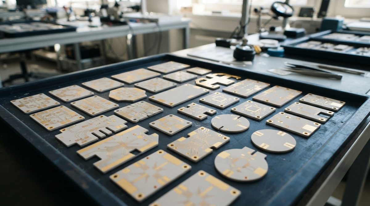
AlN costs 3–5× more per unit area than 96% alumina. If your device dissipates under 1–2 W/cm² and junction temperature has comfortable margin, alumina at 24–28 W/mK is sufficient and far cheaper. For applications demanding extreme mechanical toughness over thermal performance—such as substrates exposed to vibration or thermal shock cycling beyond 3 000 cycles—custom silicon nitride (Si₃N₄) PCBs offer flexural strength above 600 MPa, roughly double that of AlN.
AlN is also hygroscopic. Prolonged exposure to humidity without passivation degrades surface conductivity. If your operating environment is uncontrolled (outdoor telecom enclosures without hermetic sealing, for example), alumina or Si₃N₄ may be more practical.
For high-volume consumer electronics where thermal demands are moderate, aluminum-core MCPCBs at 1–3 W/mK with a fraction of the substrate cost are the standard choice.
Specifying an Aluminum Nitride AlN Custom Order
Provide these details when requesting a quote for an aluminum nitride AlN custom ceramic PCB:
- Substrate grade and purity — e.g., 170 W/mK standard or 200 W/mK high-purity.
- Dimensions and thickness — finished size in mm, thickness from the AlN substrate datasheet.
- Metallization type — DPC, DBC, or thin-film, with copper thickness and layer count.
- Surface finish — ENIG, ENEPIG, OSP, or bare copper, depending on your assembly process.
- Edge treatment — laser-scribed snap lines, full laser cut, or diamond-saw singulation.
- Quantity and delivery schedule — prototype vs. production volumes.
Frequently Asked Questions
Can AlN ceramic PCBs be soldered with standard reflow profiles?
Yes. AlN substrates with ENIG or ENEPIG finishes are compatible with SAC305 and SnPb reflow soldering using standard IPC J-STD-020 profiles. Ramp rates should stay below 3 °C/s to avoid thermal shock cracking, especially on substrates thinner than 0.25 mm.
Does AlN need a passivation layer to resist moisture?
It is strongly recommended. Unpassivated AlN reacts with moisture to form aluminum hydroxide, which degrades thermal and electrical performance over time. A thin SiO₂ or Si₃N₄ passivation layer deposited by PECVD is standard practice for non-hermetic packages.
What is the maximum panel size available for custom AlN substrates?
Most suppliers offer sintered AlN blanks up to approximately 140 mm × 190 mm. Larger assemblies require tiling multiple substrates onto a common heatsink or carrier. Check with your fabricator for current maximum dimensions.
How does AlN compare to BeO for thermal conductivity?
Beryllium oxide (BeO) reaches 250–300 W/mK, higher than AlN’s 170–200 W/mK. However, BeO dust is a confirmed human carcinogen that causes chronic beryllium disease. Regulatory restrictions (OSHA PEL of 0.2 µg/m³) and disposal costs make BeO impractical for most new designs. AlN is the preferred non-toxic alternative for high-conductivity ceramic substrates.
Is AlN suitable for multilayer ceramic PCBs?
AlN is not used in LTCC or standard HTCC multilayer processes due to its sintering atmosphere requirements (nitrogen, not air). Multilayer AlN structures exist but require specialized co-fire processing and are limited to niche RF and aerospace applications. For most multilayer needs, alumina-based HTCC or LTCC is more practical.
Next Step
If your thermal analysis points to AlN, gather your Gerber files and substrate specs, then request a quote for AlN ceramic PCBs. An applications engineer can confirm whether DPC, DBC, or thin-film metallization best fits your design and volume requirements.