Silicon nitride Si3N4 custom ceramic PCBs offer the highest fracture toughness of any commercial ceramic substrate—typically 6–7 MPa·√m versus 3–4 MPa·√m for alumina and AlN—making them the default choice when thermal cycling, mechanical shock, or large-area power modules would crack a less resilient material. Custom fabrication lets you specify exact dimensions, metallization patterns, via placement, and surface finish for your specific power electronics or EV inverter design.
Key Takeaways
- Si3N4 fracture toughness reaches 6–7 MPa·√m (ASTM C1421), roughly double that of 96% Al2O3 or AlN.
- Thermal conductivity of commercial Si3N4 substrates ranges from 70–90 W/mK, lower than AlN (170–200 W/mK) but far above alumina (24–28 W/mK).
- Si3N4 substrates survive >3,000 thermal cycles (−40 °C to +250 °C) in standard power-cycling tests, per published Kyocera and Toshiba reliability data.
- Active metal brazing (AMB) is the primary metallization process for silicon nitride Si3N4 custom substrates; DBC is not used because the required oxide interlayer does not form reliably on Si3N4.
- Custom Si3N4 PCBs cost 5–10× more than equivalent Al2O3 substrates, justified only when reliability under thermal cycling is the binding constraint.
Why Silicon Nitride Si3N4 Custom Substrates Lead in Power Electronics
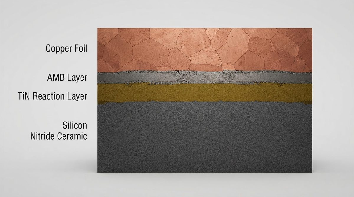
The core advantage of silicon nitride is mechanical reliability under repeated thermal stress. In a power module, the substrate endures thousands of heat-up and cool-down cycles. Each cycle induces stress at the copper-ceramic interface due to CTE mismatch. Alumina and AlN substrates eventually develop micro-cracks that propagate to failure. Si3N4’s high fracture toughness and flexural strength (600–800 MPa per ASTM C1161) resist crack propagation far longer.
This matters most in automotive traction inverters, railway power converters, and industrial motor drives where field replacement is expensive and warranty periods stretch to 10–15 years. A detailed look at Si3N4 material properties shows why the numbers favor this substrate for long-life applications.
Si3N4 Properties vs. Other Ceramic Substrates
| Parameter | Si3N4 | AlN | Al2O3 96% | Unit | Condition |
|---|---|---|---|---|---|
| Thermal conductivity | 70–90 | 170–200 | 24–28 | W/mK | 20 °C |
| Fracture toughness | 6–7 | 2.5–3.5 | 3–4 | MPa·√m | ASTM C1421 |
| Flexural strength | 600–800 | 300–400 | 300–380 | MPa | ASTM C1161, 3-pt bend |
| CTE | 2.7–3.0 | 4.5–5.0 | 6.5–7.5 | ppm/°C | 20–300 °C |
| Dielectric strength | 15–18 | 14–17 | 10–15 | kV/mm | AC, 60 Hz |
| Thermal cycle life (−40/+250 °C) | >3,000 | ~500–1,000 | ~500–800 | cycles to crack | 0.3 mm Cu, AMB/DBC |
Typical values for commercially available material, for comparison only. Confirm against the datasheet for your specific grade. Sources: Kyocera SN series datasheet; CoorsTek Ceralloy 147 datasheet; Maruwa AlN datasheet.
Silicon Nitride Si3N4 Custom Fabrication Process
Si3N4 substrates are produced by sintering silicon nitride powder with sintering aids (Y2O3, MgO) at 1,700–1,900 °C under nitrogen atmosphere. The sintered blanks are then ground and optionally polished or lapped to the required surface roughness and thickness. Ordering a silicon nitride Si3N4 custom board adds several steps beyond blank substrate production:
- Substrate sizing and scribing. Blanks are laser-scribed or diamond-scribed to the panel layout. For snap-apart designs, laser-scribed Si3N4 panels allow clean singulation without full-thickness cutting.
- Metallization by AMB. An active braze alloy (typically AgCuTi) bonds copper foil (0.3–0.8 mm) directly to the Si3N4 surface at 780–900 °C in vacuum. The titanium in the alloy reacts with the nitride surface to form a TiN bonding layer. DBC does not work reliably on Si3N4 because the process depends on a Cu-CuO eutectic that requires an oxide ceramic surface.
- Circuit patterning. Copper is etched to the desired trace geometry using standard photolithographic methods. Minimum trace/space depends on copper thickness; 0.3 mm Cu typically supports 0.3 mm trace/space.
- Surface finish. NiAu, NiPdAu, or bare Cu with OSP, depending on the solder or sintering process used for die attach.
- Electrical and dimensional inspection. Hipot testing, dimensional verification, and surface roughness measurement.
Enter your substrate dimensions, copper thickness, and target operating temperature to see how temperature derating affects your silicon nitride Si3N4 custom design margins.
Worked Example: Thermal Resistance of a Custom Si3N4 Substrate
Consider a 40 mm × 40 mm Si3N4 substrate, 0.32 mm thick, with thermal conductivity of 80 W/mK. The one-dimensional thermal resistance through the substrate is:
Rth = t / (k × A) = 0.00032 m / (80 W/mK × 0.0016 m²) = 0.0025 °C/W
For comparison, the same geometry in AlN at 180 W/mK gives 0.0011 °C/W, and in 96% Al2O3 at 26 W/mK gives 0.0077 °C/W. Si3N4 sits between the two. For a 200 W IGBT module, the substrate alone contributes 0.5 °C of temperature rise—manageable in most designs. The thermal penalty versus AlN is real but small relative to other resistances in the stack (die attach, TIM, heatsink).
Design Rules for Custom Si3N4 Boards
Substrate Thickness
Standard thicknesses are 0.25 mm, 0.32 mm, and 0.635 mm. Thinner substrates reduce thermal resistance but are harder to handle. For thin Si3N4 substrates below 0.25 mm, handling fixtures and vacuum tooling become necessary during assembly.
Copper Thickness
AMB supports copper from 0.15 mm to 0.8 mm. Thicker copper carries more current and spreads heat laterally, but increases CTE-mismatch stress. Most EV inverter designs settle on 0.3 mm as a balance point.
Panel Size
Si3N4 substrates are typically available up to 190 mm × 140 mm after metallization. Larger panels increase yield per firing but raise warpage risk. Confirm maximum panel size with your supplier early in the design phase.
When NOT to Use Si3N4
Silicon nitride Si3N4 custom substrates are overkill and overpriced for many applications. Choose a different substrate when:
- Thermal cycling is mild (<500 cycles, ΔT <150 °C). Al2O3 or AlN with DBC will survive and cost far less. Compare options across ceramic PCB materials.
- Maximum thermal conductivity is the binding constraint. AlN at 170–200 W/mK outperforms Si3N4 by roughly 2×. If your thermal model shows the substrate is the bottleneck, AlN wins.
- Budget is tight and volumes are high. Si3N4 substrates cost 5–10× more than Al2O3. For consumer LED modules or low-power RF, the cost cannot be justified.
- Operating temperature stays below 150 °C and loads are static. FR-4 or metal-core PCBs handle this at a fraction of the price.
Frequently Asked Questions
Can I get Si3N4 substrates with DBC instead of AMB?
No. DBC (direct bonded copper) relies on a copper-oxide eutectic that bonds to oxide ceramics like Al2O3 and AlN. Si3N4 is a nitride, so the oxide interlayer does not form reliably. AMB with an active titanium-bearing braze alloy is the standard metallization method for Si3N4.
What is the maximum continuous operating temperature for a Si3N4 PCB?
The ceramic itself is stable above 1,000 °C in inert atmosphere. The practical limit is set by the AMB braze joint and copper oxidation, which restrict continuous use to about 300–350 °C in most designs. Junction temperatures in power modules rarely exceed 200 °C, well within this range.
How does Si3N4 compare across different sintering-aid grades?
Sintering aids (Y2O3 vs. MgSiN2, for example) affect grain boundary phases and therefore thermal conductivity. High-thermal-conductivity grades (85–90 W/mK) use optimized sintering chemistries to reduce phonon scattering at grain boundaries. Lower-cost grades may only reach 70 W/mK. Always request the specific grade’s datasheet.
What minimum order quantity is typical for silicon nitride Si3N4 custom PCBs?
MOQ depends on the supplier and the complexity of the AMB pattern. Prototype runs of 5–25 pieces are common. Production orders typically start at 100–500 substrates per design to amortize tooling and setup costs.
Is Si3N4 suitable for RF or high-frequency circuits?
Si3N4 has a dielectric constant of approximately 7–8 at 1 MHz, which is acceptable for some RF applications but higher than alumina (9.0–9.8) and much higher than PTFE-based laminates (2.1–3.5). For millimeter-wave designs, PTFE or quartz substrates are usually preferred. Si3N4’s strength lies in power electronics, not RF.
Next Step
If your design involves high-reliability power modules, EV inverters, or any application where thermal cycling drives substrate failure, a silicon nitride Si3N4 custom substrate with AMB metallization is worth the cost premium. Download the Si3N4 substrate datasheet to verify that the properties match your thermal model, then request a quote with your panel dimensions and copper thickness requirements.