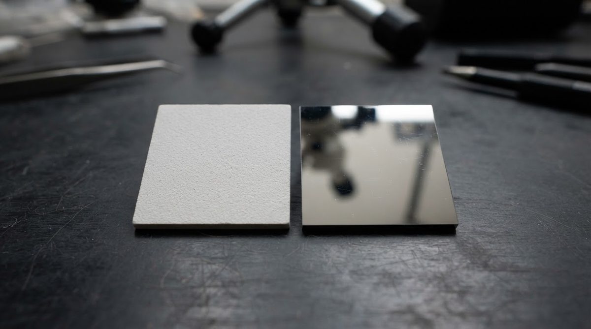
An alumina 96% Al2O3 polished substrate delivers a surface roughness of Ra ≤0.1 µm (typical 0.02–0.05 µm after optical polish), compared with Ra 0.4–0.8 µm for an as-fired surface. That smoother finish matters for thin-film metallisation, laser trimming, hermetic sealing, and any process where film adhesion and line definition depend on sub-micron flatness. Choosing alumina 96% Al2O3 polished material does add cost: polishing increases the unit price by 20–40% versus an as-fired substrate of the same dimensions.
What “Polished” and “Lapped” Actually Mean for Alumina 96% Al2O3
The two terms are often used interchangeably in supplier catalogs, but they describe different steps. Lapping uses a fixed-abrasive or loose-abrasive process to bring the substrate to a controlled thickness and flatness, typically achieving Ra 0.1–0.25 µm. Polishing follows lapping and uses progressively finer slurries (often colloidal silica or diamond) to push roughness below Ra 0.05 µm. A substrate sold as “polished/lapped” has gone through both stages.
For thick-film processes such as screen-printed silver or gold conductors, a lapped finish (Ra ≤0.25 µm) is usually sufficient. Thin-film sputtering or evaporation of NiCr, TaN, or Ti/Pt/Au demands the full optical polish to prevent pinholes and ensure ±1% resistor tolerance, per guidance in MIL-PRF-55342.
Key Properties of Alumina 96% Al2O3 Polished Substrates
| Parameter | Value | Unit | Condition | Source |
|---|---|---|---|---|
| Al2O3 purity | 96 ± 0.5 | % | By weight | CoorsTek ADS-996 datasheet |
| Thermal conductivity | 24–28 | W/m·K | 20 °C, ASTM E1461 | Kyocera A-493 datasheet |
| Dielectric constant (εr) | 9.0–9.5 | — | 1 MHz, 25 °C | CoorsTek ADS-996 |
| Dielectric strength | 14–16 | kV/mm | AC, 60 Hz, ASTM D149 | Kyocera A-493 |
| Flexural strength | 330–380 | MPa | ASTM C1161, 4-pt bend | CeramTec Rubalit 710 |
| CTE | 7.1–7.4 | ppm/°C | 25–300 °C | CoorsTek ADS-996 |
| Surface roughness (polished) | 0.02–0.05 | µm Ra | Optical polish, profilometry | Maruwa HA-96 datasheet |
| Surface roughness (as-fired) | 0.4–0.8 | µm Ra | Profilometry | Maruwa HA-96 |
| Volume resistivity | >10¹⁴ | Ω·cm | 25 °C | CoorsTek ADS-996 |
Typical values for commercially available material, for comparison only. Confirm against the datasheet for your specific grade.
The 4% glass-phase binder in 96% alumina lowers thermal conductivity relative to 99.6% alumina polished substrates, which reach 28–35 W/m·K. It also slightly increases dielectric loss (tan δ ~0.0005 at 1 MHz vs ~0.0001 for 99.6%). For most power and sensor applications, alumina 96% Al2O3 polished is the cost-effective choice. For microwave circuits above 10 GHz or precision thin-film resistor networks, the higher-purity grade pays for itself in yield.
Why Surface Finish Matters for Metallisation
Thin-film resistors and conductors deposited by sputtering are typically 50–500 nm thick. A surface peak taller than the film itself creates a discontinuity. On an as-fired 96% alumina surface (Ra ~0.6 µm), peak-to-valley heights of 3–5 µm are common. That is an order of magnitude larger than a 200 nm TaN resistor film. The result: open circuits, resistance drift, and poor trimming accuracy.
Polishing the substrate to Ra ≤0.05 µm reduces Rz (peak-to-valley) to roughly 0.2–0.4 µm, keeping surface features well below the film thickness. This is why virtually all thin-film hybrid manufacturers specify alumina 96% Al2O3 polished substrates. For ceramic dielectric performance, the smoother interface also reduces parasitic capacitance variation in high-frequency circuits.
Polished 96% vs Polished 99.6%: Which Grade Do You Need?
| Criterion | 96% Al2O3 Polished | 99.6% Al2O3 Polished |
|---|---|---|
| Thermal conductivity | 24–28 W/m·K | 28–35 W/m·K |
| Dielectric loss (1 MHz) | ~0.0005 | ~0.0001 |
| Flexural strength | 330–380 MPa | 350–400 MPa |
| Achievable Ra | 0.02–0.05 µm | 0.01–0.03 µm |
| Relative cost | 1× | 1.5–2× |
| Best for | Thick-film hybrids, sensors, LED submounts | Thin-film precision resistors, mmWave, hermetic packages |
Typical values for commercially available material, for comparison only. Confirm against the datasheet for your specific grade.
If your design uses screen-printed conductors and operates below 6 GHz, alumina 96% Al2O3 polished is almost always the right pick. The glass phase in 96% alumina actually improves thick-film paste adhesion during firing. For thin-film networks requiring ±0.1% post-trim tolerance, or for frequencies above 10 GHz where tan δ drives insertion loss, move to 99.6% alumina PCBs.
Use the tool below to compare thermal derating across alumina grades and see how substrate thickness and power density interact for your specific design.
Typical Tolerances for Alumina 96% Al2O3 Polished Substrates
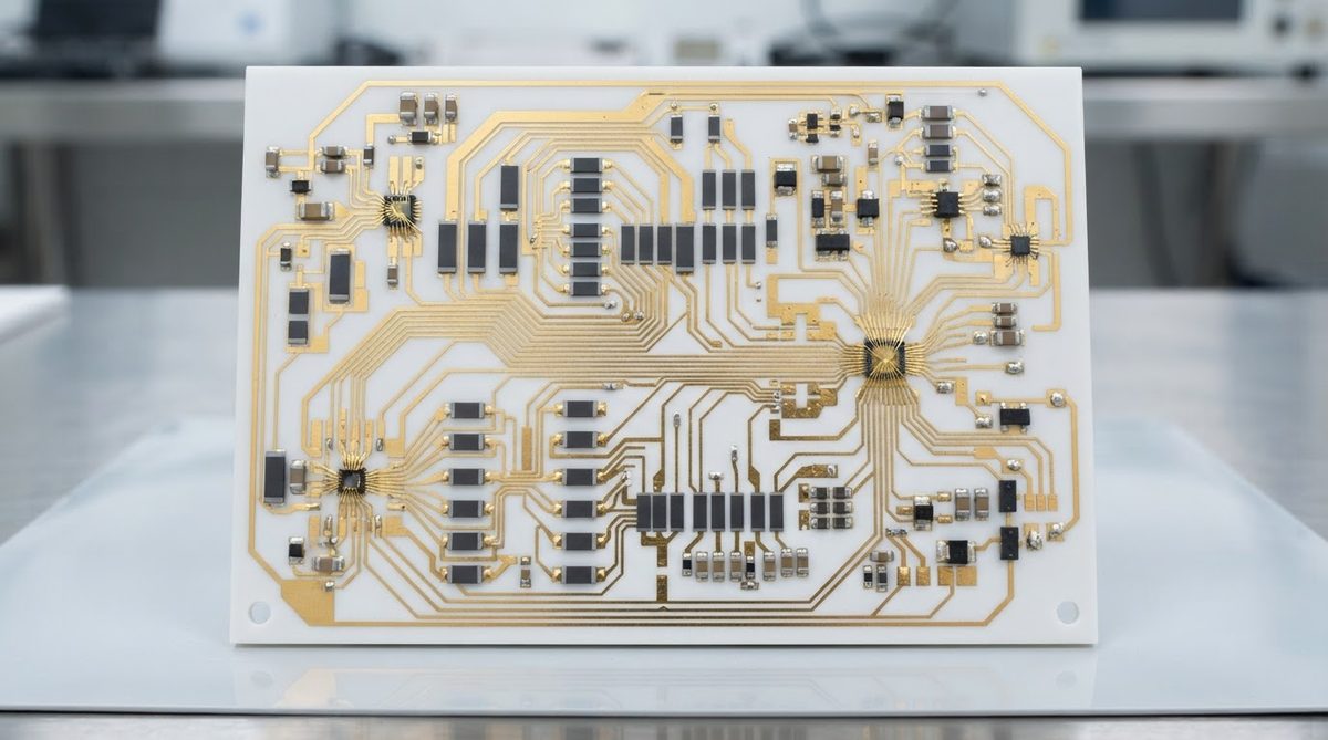
Lapping and polishing tighten the thickness tolerance significantly compared with as-fired substrates. Expect the following from most qualified suppliers:
- Thickness tolerance: ±0.013 mm (±0.5 mil) after lapping, vs ±0.05 mm as-fired.
- TTV (total thickness variation): ≤0.010 mm across a 50 × 50 mm substrate.
- Flatness (bow/warp): ≤0.05 mm over 50 mm, per ASTM F657.
- Length/width: ±0.13 mm (laser-scribed or diamond-sawn edges).
Tighter TTV is critical for wire-bond die attach, where coplanarity affects loop height consistency. If your package requires TTV below 5 µm, discuss it with your supplier before committing to 96%; the glass-phase grain structure makes ultra-flat polishing harder than on 99.6% material.
When Not to Use Polished 96% Alumina
You need higher thermal conductivity. At 24–28 W/m·K, 96% alumina is adequate for moderate power densities. For power modules dissipating more than ~50 W/cm², consider polished aluminum nitride (AlN) at 170–200 W/m·K.
You need mechanical toughness more than thermal performance. 96% alumina is brittle (K_IC ~3.5 MPa·m^½). If your substrate will see mechanical shock or vibration beyond what a rigid mount can absorb, polished silicon nitride (Si3N4) offers fracture toughness of 6–7 MPa·m^½.
Your process is entirely thick-film. Polishing is an added cost that improves thick-film performance only marginally. An as-fired or lapped surface is usually sufficient for screen-printed conductors with line widths above 100 µm.
Your volumes justify bulk pricing on as-fired substrates. For high-volume sensor or LED applications where thin-film metallisation is not required, 96% alumina wholesale substrates in as-fired finish offer the lowest per-unit cost.
Frequently Asked Questions
Can I solder directly to a polished 96% alumina surface?
No. Bare alumina is not wettable by solder. You need a metallisation layer first, typically thick-film Ag/Pd or thin-film Ti/Pt/Au, followed by a solderable finish such as ENIG or tin plating. The polished surface itself does not change solderability; it affects metallisation quality.
Does polishing weaken the substrate?
Polishing can slightly reduce flexural strength by 5–10% if aggressive lapping introduces subsurface micro-cracks. A well-controlled polish with fine diamond slurry actually improves effective strength by removing as-fired surface flaws. Specify a final anneal step if your application is strength-critical.
What is the maximum substrate size available in polished 96% alumina?
Most suppliers offer alumina 96% Al2O3 polished substrates up to 114 × 114 mm (4.5″ × 4.5″) as standard. Larger panels up to ~150 × 150 mm are available but with looser flatness tolerances due to the difficulty of maintaining uniform pressure during lapping.
How do I specify surface finish on a drawing?
Call out Ra and the measurement method. A typical note reads: “Surface finish: Ra ≤0.05 µm per ISO 4287, measured with stylus profilometer, 0.8 mm cutoff length.” Also specify which side(s) require polishing; single-side polish is cheaper than double-side.
Is polished 96% alumina suitable for DBC (Direct Bond Copper)?
Yes, but the polished surface is not required for DBC. The copper bonding process involves a Cu-O eutectic at ~1065 °C that wets the alumina grain structure. An as-fired surface works well for DBC. Polishing adds cost without improving bond strength in this case.