Alumina 99.6% Al2O3 polished substrates deliver surface roughness as low as Ra 0.02–0.05 µm, making them the standard choice for thin-film metallisation, hybrid microelectronics, and precision sensor platforms where sub-micron line definition matters. Compared with as-fired 96% alumina (Ra 0.4–0.8 µm), the polished 99.6% grade gives you tighter trace geometry, lower dielectric loss, and better thermal conductivity in a single upgrade.
Key Takeaways
- 99.6% Al2O3 polished substrates reach Ra ≤0.05 µm after lapping and final polish, per CoorsTek ADS-996 datasheet.
- Thermal conductivity is 33–36 W/mK at 25 °C, roughly 30–40 % higher than 96% alumina (24–28 W/mK).
- Dielectric constant is 9.7–9.9 at 1 MHz (ASTM D150), with loss tangent below 0.0002 at 1 MHz.
- Typical thickness range for polished substrates is 0.25–2.0 mm; thinner stock requires lapping before polish.
- Cost runs 2–4× that of as-fired 96% alumina, driven by raw-material purity and the multi-step finishing process.
What Makes 99.6% Alumina Different from 96%?
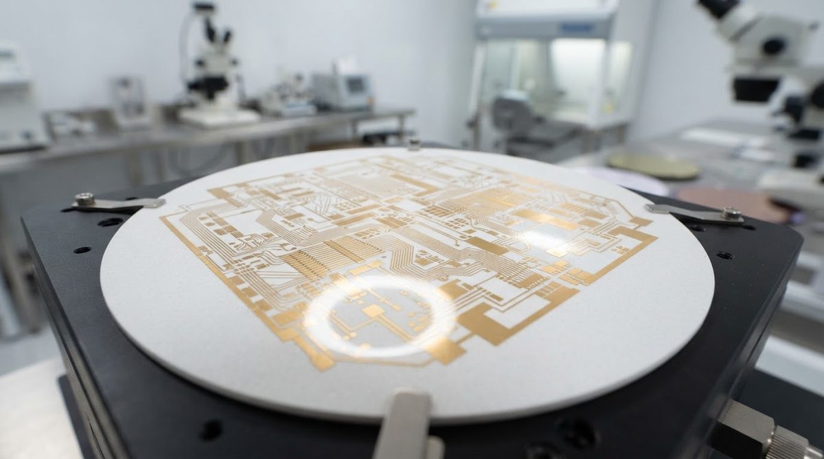
The 3.6 percentage-point jump in purity removes most of the glassy silicate phase used as a sintering aid in 96% grades. Less glass phase means higher grain density, which improves thermal conductivity, raises the flexural strength ceiling, and lowers dielectric loss. For RF and thin-film circuits, the reduced glass content also stabilises the dielectric constant across temperature and frequency.
The trade-off is machinability. With less glass binder, 99.6% alumina is harder (HV 1500–1600 vs. HV 1300–1400 for 96%) and more abrasive on tooling. Laser scribing and diamond grinding are the practical shaping methods. If your design needs complex routed outlines or many through-holes, factor in longer machining time and higher per-piece cost. For a broader comparison across ceramic grades, see the guide on choosing the right ceramic substrate.
Surface Finish Grades: As-Fired, Lapped, and Polished
Not every “polished” substrate is the same. The industry uses three finish levels, each suited to different metallisation methods.
| Finish | Typical Ra (µm) | Method | Primary Use |
|---|---|---|---|
| As-fired | 0.4–0.8 | Sintered, no post-processing | Thick-film printing, general packaging |
| Lapped | 0.10–0.25 | Flat-lapping with diamond slurry | Sputtered thin-film, chip-on-board |
| Polished | 0.02–0.05 | Multi-stage CMP or fine diamond polish | Precision thin-film resistors, MEMS carriers, laser diode submounts |
Typical values for commercially available material, for comparison only. Confirm against the datasheet for your specific grade.
Polishing adds cost but is non-negotiable for sputtered or evaporated thin-film circuits. Surface defects at the 0.1 µm scale cause pinholes in metal layers only a few hundred nanometres thick, leading to open circuits or localised hot spots. If your metallisation is screen-printed thick film (10–25 µm conductor), lapped finish is usually sufficient and saves 15–25 % on substrate cost.
Material Properties at a Glance
| Parameter | Value | Unit | Condition | Source |
|---|---|---|---|---|
| Al2O3 purity | 99.6 | % | — | CoorsTek ADS-996 |
| Density | 3.89–3.92 | g/cm³ | ASTM C373 | CoorsTek ADS-996 |
| Thermal conductivity | 33–36 | W/mK | 25 °C, ASTM E1461 | Kyocera A-493 |
| CTE | 7.9–8.2 | ppm/°C | 25–400 °C | CoorsTek ADS-996 |
| Flexural strength | 380–450 | MPa | ASTM C1161, 4-pt bend | CoorsTek ADS-996 |
| Dielectric constant (εr) | 9.7–9.9 | — | 1 MHz, ASTM D150 | Kyocera A-493 |
| Loss tangent (tan δ) | <0.0002 | — | 1 MHz, ASTM D150 | Kyocera A-493 |
| Dielectric strength | ≥16 | kV/mm | ASTM D149 | CoorsTek ADS-996 |
| Surface roughness (polished) | 0.02–0.05 | µm Ra | After CMP | Maruwa HA-series |
Typical values for commercially available material, for comparison only. Confirm against the datasheet for your specific grade.
For a deeper look at how dielectric constant and loss tangent affect high-frequency designs, see ceramic substrate dielectric properties.
Where 99.6% Alumina Polished Substrates Excel
Thin-film hybrid circuits. Sputtered NiCr or TaN resistor networks on polished 99.6% alumina achieve ±0.1 % tolerance after laser trimming. The low Ra prevents micro-cracks in the resistor film that would drift under thermal cycling.
Laser diode and LED submounts. The CTE of 99.6% alumina (7.9–8.2 ppm/°C) sits between GaAs (5.7) and copper (17), providing a reasonable compromise for die attach. Polished surfaces ensure uniform solder wetting across the bond pad.
MEMS and sensor carriers. Flatness and parallelism matter when a MEMS die is epoxy-bonded. Polished 99.6% alumina substrates are routinely held to total thickness variation (TTV) below 5 µm across a 25 × 25 mm coupon.
High-reliability thick-film circuits. Medical implant electronics and aerospace instrumentation often specify 99.6% purity for its lower ionic impurity content, which reduces long-term drift in resistor and conductor films.
When NOT to Use 99.6% Alumina Polished
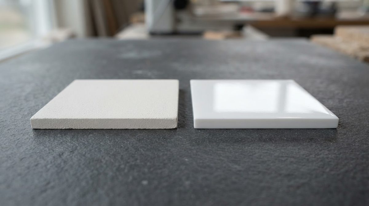
High-power modules above ~50 W/cm². At serious heat flux densities, 33–36 W/mK is not enough. Aluminum nitride polished substrates at 170–200 W/mK handle that range far better.
Mechanically stressed assemblies. If the substrate will see repeated flexure or mechanical shock, silicon nitride polished substrates offer 600–800 MPa flexural strength and much higher fracture toughness (6–7 MPa·√m vs. 3.5–4 for alumina).
Cost-sensitive, high-volume consumer products. Standard 96% alumina or even FR-4 metal-core boards will do the job at a fraction of the price when thin-film precision is not required.
Complex multilayer routing. Alumina substrates are single- or double-sided. If you need 4+ layers with buried vias, LTCC or organic HDI is the better architecture.
Worked Example: Thermal Resistance of a Polished 99.6% Al2O3 Submount
Suppose you are mounting a 2 W laser diode on a 10 × 10 × 0.5 mm polished 99.6% alumina submount. A quick one-dimensional estimate of substrate thermal resistance:
Rth = t / (k × A)
where t = 0.5 mm = 0.0005 m, k = 35 W/mK, A = 10 × 10 mm = 0.0001 m².
Rth = 0.0005 / (35 × 0.0001) = 0.143 °C/W
At 2 W dissipation, the temperature drop across the substrate is 0.29 °C. For most laser diode applications this is negligible; the solder joint and heat-sink interface dominate the thermal stack.
If the same submount were 96% alumina (k ≈ 26 W/mK), Rth rises to 0.192 °C/W — still small, but the 99.6% grade gives a 26 % improvement that compounds when you stack multiple thermal interfaces.
Frequently Asked Questions
Can I get 99.6% alumina polished on both sides?
Yes. Double-side polished (DSP) substrates are standard catalogue items from most ceramic suppliers. Specify DSP explicitly; single-side polish (SSP) is the default on many order forms.
What thickness is available for polished 99.6% alumina?
Common stock thicknesses are 0.25, 0.38, 0.50, 0.635, and 1.0 mm. Thicker blanks up to 2.0 mm are available but less commonly polished. Below 0.25 mm, handling breakage rises sharply and pricing increases.
Does polishing affect the dielectric strength?
Polishing can slightly improve dielectric strength by removing surface flaws that act as initiation sites for electrical breakdown. Measured values on polished coupons are typically at the upper end of the 16–20 kV/mm range reported for 99.6% alumina.
How does 99.6% alumina compare to AlN for thin-film circuits?
AlN offers 5–6× higher thermal conductivity but a lower dielectric constant (8.5–8.9 vs. 9.7–9.9) and higher raw-material cost. For thin-film circuits where thermal load is moderate and cost matters, 99.6% alumina is the more economical choice. When heat flux exceeds roughly 30 W/cm², AlN becomes necessary.
Is 99.6% alumina biocompatible?
High-purity alumina is widely used in medical implants (hip joints, dental posts) and is considered biocompatible per ISO 6474. For implantable electronics, the substrate itself is not the limiting factor; encapsulation and hermetic sealing are the design challenges.
Next Step
If 99.6% alumina polished substrates fit your project, review 99.6% alumina wholesale options and lead times for volume pricing. For projects still in the material-selection phase, the ceramic substrate selection guide walks through the full decision tree.