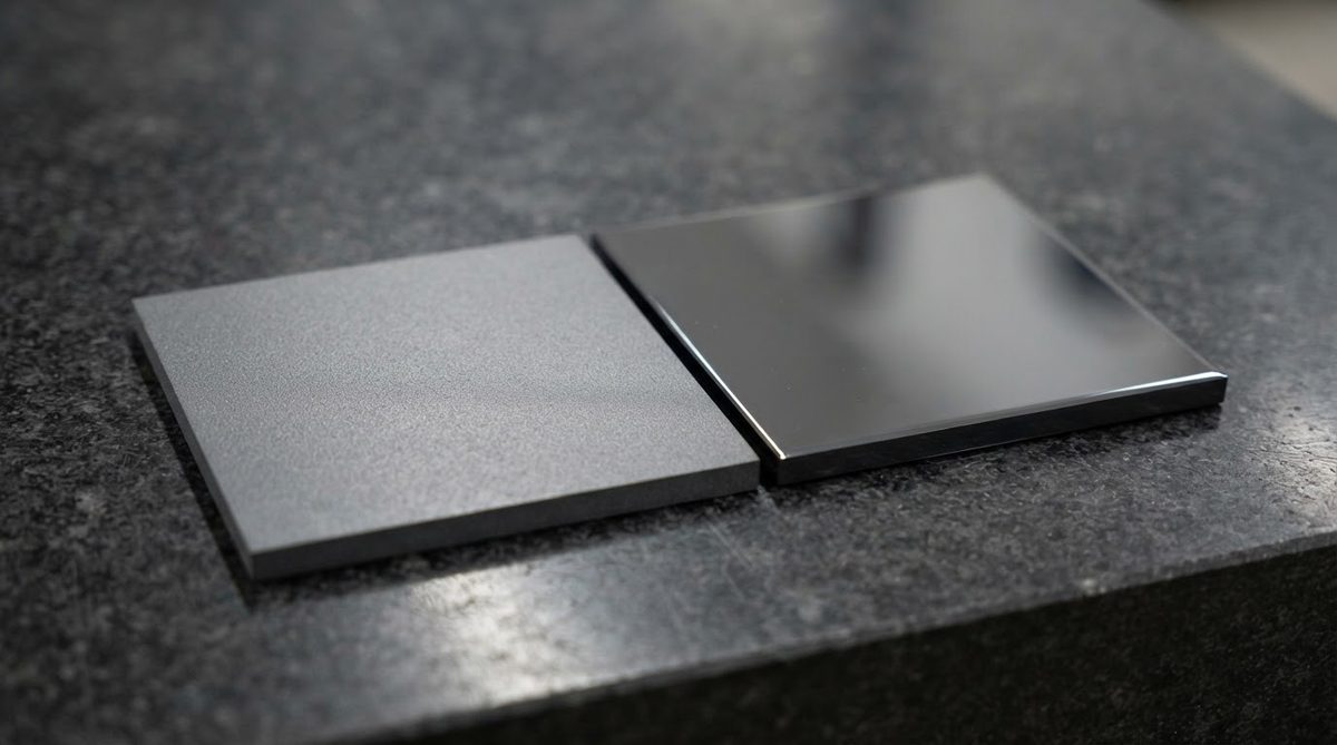
A silicon nitride Si3N4 polished substrate achieves surface roughness values from Ra 0.3 µm (standard lapped) down to Ra 0.01 µm (optical-grade polish), making it the preferred ceramic for applications where bond-line thickness, die-attach voiding, and metallization adhesion are tightly controlled. The combination of Si3N4’s exceptional fracture toughness (6–7 MPa·√m per ASTM C1421) and a mirror finish gives designers a substrate that survives thermal cycling while meeting the flatness demands of AMB, DBC, and thin-film metallization.
What “Polished” and “Lapped” Mean for Silicon Nitride Si3N4 Polished Substrates
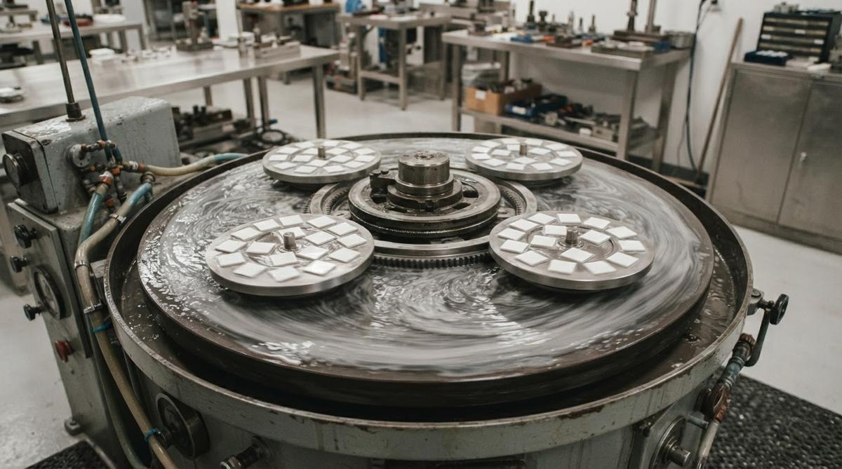
Lapping and polishing are distinct steps. Lapping uses a free abrasive slurry (typically alumina or diamond particles, 9–15 µm) on a cast-iron or glass plate to flatten the substrate and bring roughness into the Ra 0.2–0.5 µm range. Polishing follows with finer abrasive (colloidal silica or diamond paste, 0.25–3 µm) on a compliant pad to push roughness below Ra 0.1 µm. Both processes remove material—usually 10–50 µm per side—so starting thickness must account for stock removal.
For most power-module substrates bonded via Si3N4 AMB active metal brazing, a lapped finish of Ra 0.2–0.4 µm is sufficient because the braze filler (typically Ag-Cu-Ti, 10–20 µm thick) fills minor surface irregularities. Thin-film sputtered metallization, on the other hand, requires a silicon nitride Si3N4 polished surface with Ra < 0.05 µm to avoid pinholes and adhesion failures. Choosing the right finish grade saves cost: a lapped substrate can be 30–50 % less expensive than a fully polished one.
Surface Roughness Grades for Silicon Nitride Si3N4 Polished and Lapped Finishes
| Finish grade | Ra (µm) | Rz (µm) | Typical use | Source |
|---|---|---|---|---|
| As-fired | 0.8–1.5 | 5–10 | Structural, non-bonded | Kyocera SN282 datasheet |
| Standard lapped | 0.2–0.5 | 1.5–3.5 | DBC / AMB bonding | Maruwa SN-90 datasheet |
| Fine lapped | 0.05–0.15 | 0.4–1.0 | Thick-film printing, solder preforms | CoorsTek Cerapure data |
| Polished | 0.01–0.05 | 0.1–0.3 | Thin-film metallization, RF, optical | Toshiba Materials TSN-03NH |
Typical values for commercially available material, for comparison only. Confirm against the datasheet for your specific grade.
Why Surface Finish Matters for Copper Bonding
In Si3N4 DBC (direct bonded copper) processes, a Cu-O eutectic wets the ceramic surface at roughly 1065 °C. Peaks and valleys on a rough surface trap gas pockets that become voids under the copper layer. Voids larger than 2–3 % of the bond area raise local thermal resistance and concentrate mechanical stress during thermal cycling (per Infineon AN2019-05 on power module reliability). A lapped surface at Ra ≤ 0.3 µm keeps void fraction below 1 % in production.
AMB brazing is somewhat more tolerant because the braze alloy is thicker, but substrates rougher than Ra 0.5 µm still show measurably higher peel-strength scatter. If your design targets >200 N/cm peel strength (a common automotive spec), specify Ra ≤ 0.3 µm. For thin-film circuits requiring sputtered Ti/Cu or Cr/Cu seed layers, only a silicon nitride Si3N4 polished finish at Ra ≤ 0.05 µm delivers the pinhole-free adhesion needed for reliable sub-10 µm traces.
Worked Example: Choosing a Finish for an EV Inverter Substrate
Suppose you are specifying a 0.32 mm thick Si3N4 substrate for a 200 A SiC half-bridge module. The Si3N4 thermal conductivity for your chosen grade is 90 W/mK. The die is soldered to 0.3 mm Cu bonded by AMB.
- Bond quality target: <2 % void area per SAT inspection → requires Ra ≤ 0.3 µm.
- Metallization type: AMB (Ag-Cu-Ti braze, ~15 µm) → lapped finish is adequate; a full silicon nitride Si3N4 polished surface adds cost with no reliability gain for this bonding method.
- Flatness tolerance: ±10 µm TTV (total thickness variation) across 50 × 50 mm → achievable with double-side lapping on a planetary machine.
- Stock removal budget: Starting blank at 0.38 mm, removing ~30 µm per side, yielding 0.32 ± 0.01 mm → order Si3N4 thin substrates at 0.38 mm pre-lap thickness.
Result: specify “double-side lapped, Ra ≤ 0.3 µm, TTV ≤ 10 µm.” This avoids the 30–50 % premium of a polished finish while meeting bond and thermal targets.
Enter your substrate dimensions, target roughness grade, and quantity below to see how finish selection affects estimated pricing.
Key Material Properties of Silicon Nitride Si3N4 Polished Substrates
Polishing does not change bulk properties, but it does affect surface flaw population, which in turn affects flexural strength. A silicon nitride Si3N4 polished substrate typically tests 50–100 MPa higher in four-point bend (per ASTM C1161) than an as-fired one because surface flaws—the usual crack-initiation sites—are removed.
| Property | Value | Unit | Condition | Source |
|---|---|---|---|---|
| Flexural strength (as-fired) | 600–800 | MPa | 4-pt bend, RT, ASTM C1161 | Kyocera SN282 |
| Flexural strength (polished) | 700–900 | MPa | 4-pt bend, RT, ASTM C1161 | Toshiba TSN-03NH |
| Fracture toughness | 6–7 | MPa·√m | SEVNB, RT, ASTM C1421 | CoorsTek SC-211 |
| Thermal conductivity | 70–90 | W/mK | Laser flash, 25 °C | Maruwa SN-90 |
| Dielectric strength | 15–17 | kV/mm | IEC 60672 | Kyocera SN282 |
| CTE | 2.5–3.2 | ppm/K | RT–400 °C | Maruwa SN-90 |
Typical values for commercially available material, for comparison only. Confirm against the datasheet for your specific grade.
When Not to Use Silicon Nitride Si3N4 Polished Substrates
Cost-sensitive, lower-power designs. If your thermal load stays below 50 W/cm² and the module sees fewer than 5,000 thermal cycles, 96 % alumina (Al₂O₃) with a standard lapped finish at roughly one-fifth the substrate cost is the practical choice. See the full ceramic substrate material comparison for a side-by-side breakdown.
As-fired is good enough. For structural spacers, sensor housings, or any non-bonded application, paying for lapping or polishing adds cost with zero functional benefit.
Aluminum nitride (AlN) at higher thermal loads. When thermal conductivity above 150 W/mK is the primary driver and the module does not need extreme thermal-cycle endurance, polished AlN may outperform Si3N4 thermally at a lower price per substrate.
FAQ
Does polishing weaken a Si3N4 substrate?
No. Polishing removes surface flaws that initiate cracks, so flexural strength typically increases by 50–100 MPa compared to as-fired surfaces. Bulk fracture toughness (6–7 MPa·√m) is unaffected by surface finishing.
What surface roughness do I need for AMB brazing?
Ra ≤ 0.3 µm (standard lapped) is sufficient for most AMB processes using Ag-Cu-Ti braze alloys. Going finer than Ra 0.1 µm for AMB adds cost without measurable improvement in peel strength or void fraction.
Can I get single-side polish on Si3N4?
Yes. Single-side lapping or polishing is standard practice when only one face receives metallization. The unpolished side retains the as-fired or blanchard-ground finish, reducing processing time and cost by roughly 20–30 %.
How much thickness do I lose to lapping and polishing?
Expect 10–50 µm of stock removal per side depending on starting roughness and target Ra. Order blanks 40–100 µm thicker than your finished spec to account for this. Specify your final thickness and TTV on the drawing; the supplier will select the correct starting blank.
Is polished Si3N4 available below 0.2 mm thickness?
It is, but handling fragility rises sharply below 0.2 mm even with Si3N4’s high toughness. Substrates at 0.15–0.20 mm are produced for specific IGBT and SiC module platforms. Discuss yield expectations with your supplier before committing to volume.
What inspection method verifies surface roughness?
Contact profilometry (stylus, per ISO 4287) is the standard production method. White-light interferometry (per ISO 25178) gives areal roughness data (Sa) and is preferred for silicon nitride Si3N4 polished surfaces below Ra 0.05 µm where stylus tip radius limits resolution.
For volume pricing on lapped or polished Si3N4 substrates, visit the Si3N4 substrate purchasing page or request a quote with your thickness, roughness, and quantity requirements.