96% alumina (Al₂O₃) is the default ceramic PCB substrate for most applications that need better thermal or electrical performance than FR-4 but do not require the cost premium of aluminum nitride or 99.6% alumina. It offers thermal conductivity of 24–28 W/m·K at 25 °C, dielectric strength above 10 kV/mm, and flexural strength of 350–380 MPa (per ASTM C1161) — all at roughly one-third the per-unit cost of AlN.
Key Takeaways
- 96% alumina substrates conduct heat at 24–28 W/m·K (25 °C), about 100× better than standard FR-4 (0.25 W/m·K).
- Dielectric constant sits at 9.0–9.5 at 1 MHz, making it suitable for power isolation but less ideal for high-frequency RF above ~20 GHz.
- Custom fabrication routes include thick film, thin film (DPC), DBC, HTCC, and LTCC — each with different trace resolution and temperature limits.
- Typical as-fired surface roughness is 0.5–1.0 µm Ra; polished substrates can reach below 0.1 µm Ra for thin-film metallization.
- 96% alumina is brittle. Design for mechanical shock requires minimum edge-to-hole clearance of 2× substrate thickness and radiused internal corners.
Material Properties of 96% Al₂O₃
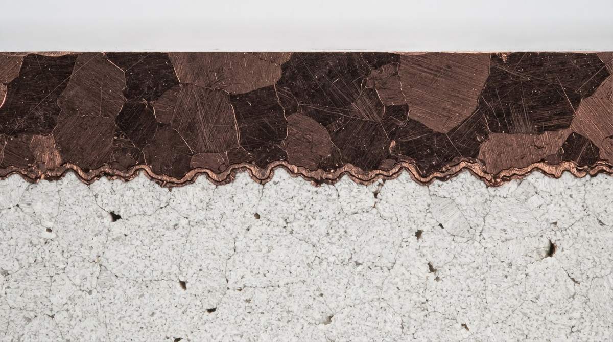
The 4% non-alumina content in a 96% substrate is mostly a silica-based glass phase that acts as a sintering aid. This glass phase lowers the firing temperature (to ~1,600 °C vs. ~1,700 °C for 99.6%) and reduces cost, but it also slightly reduces thermal conductivity and increases dielectric loss compared to higher-purity grades. For a full breakdown of measured values, see the alumina 96% material properties reference.
| Parameter | Value | Unit | Condition | Source |
|---|---|---|---|---|
| Thermal conductivity | 24–28 | W/m·K | 25 °C | CoorsTek ADS-96R datasheet |
| CTE | 7.2–8.2 | ppm/°C | 25–300 °C | Kyocera A-476 datasheet |
| Dielectric constant (εr) | 9.0–9.5 | — | 1 MHz, 25 °C | CoorsTek ADS-96R |
| Dielectric strength | 10–15 | kV/mm | AC, 60 Hz | CeramTec Rubalit 708S |
| Flexural strength | 350–380 | MPa | 4-pt bend, ASTM C1161 | CoorsTek ADS-96R |
| Volume resistivity | >10¹⁴ | Ω·cm | 25 °C | Kyocera A-476 |
| Max continuous use temp. | 1,000+ | °C | In inert/oxidizing atmosphere | General ceramic literature |
Typical values for commercially available material, for comparison only. Confirm against the datasheet for your specific grade.
Custom Fabrication Processes for 96% Alumina PCBs
The choice of metallization process determines your minimum feature size, copper thickness, and cost per board. Here is how the main options compare on a 96% alumina substrate.
Thick Film
Screen-printed conductors (Ag, AgPd, Au) fired at 850–950 °C. Line/space resolution is typically 100–150 µm. This is the lowest-cost route for moderate-density circuits and resistor networks. Conductor thickness is limited to roughly 10–25 µm per print pass.
Thin Film / DPC (Direct Plated Copper)
Sputtered seed layers followed by photolithographic patterning and electroplating. Achieves line/space down to 20–50 µm and copper thickness of 1–200 µm. Best for high-density interconnects and precision resistor trimming. Surface roughness of the substrate matters here — a lapped surface below 0.25 µm Ra improves adhesion and etch uniformity. For details on roughness grades, see alumina 96% surface finish and roughness.
DBC (Direct Bond Copper)
Copper foil (typically 0.127–0.635 mm) bonded directly to the alumina at ~1,065 °C using a controlled Cu-O eutectic. High current-carrying capacity for power modules. Minimum pattern features are coarser — around 200–300 µm — but copper can handle 50+ A continuous per trace depending on width.
HTCC and LTCC
Co-fired multilayer processes. HTCC fires at ~1,500 °C with refractory metals (W, Mo); LTCC fires at ~850 °C with Ag or Au. Both allow embedded vias and internal routing, but LTCC uses a different glass-ceramic tape body, not a pure 96% alumina. HTCC can use 96% alumina tape. These processes suit multilayer sensor packages and hybrid modules.
Design Considerations for Custom 96% Alumina Boards
Ceramic substrates do not behave like FR-4 laminates. Three areas catch engineers off guard most often.
Mechanical fragility. 96% alumina has high compressive strength (~2,000 MPa) but is brittle under tension and impact. Avoid sharp internal corners — use a minimum fillet radius of 0.3 mm. Keep holes at least 2× the substrate thickness from any edge. Panel singulation by laser scribing or diamond dicing is preferred over V-scoring, which can propagate micro-cracks. More on this at laser machining of alumina 96% substrates.
CTE mismatch. At 7.2–8.2 ppm/°C, 96% alumina is a reasonable match for silicon (2.6 ppm/°C) through a solder joint, but a poor match for standard PCB laminates (~14–17 ppm/°C). If the ceramic board plugs into a larger FR-4 system, use compliant interconnects or flexible leads to absorb differential expansion.
Thermal vias are not always needed. Because the substrate itself conducts 24–28 W/m·K, many single-layer designs can spread heat laterally through the ceramic without thermal vias. A quick sanity check: for a 1 W heat source on a 0.635 mm thick, 25 × 25 mm substrate, steady-state thermal resistance through the thickness is roughly Rth = t / (k × A) = 0.000635 / (26 × 0.000625) ≈ 0.039 °C/W — negligible. The bottleneck is almost always the interface to the heatsink, not the ceramic.
96% Alumina vs. Higher-Purity and Alternative Substrates
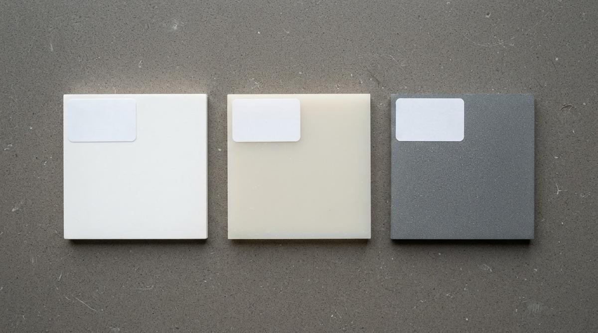
If 96% alumina does not quite meet your thermal or frequency requirements, the next step up is usually 99.6% alumina or aluminum nitride. The table below puts the key differences side by side.
| Parameter | 96% Al₂O₃ | 99.6% Al₂O₃ | AlN | Unit / Condition |
|---|---|---|---|---|
| Thermal conductivity | 24–28 | 28–35 | 170–200 | W/m·K, 25 °C |
| Dielectric constant | 9.0–9.5 | 9.7–9.9 | 8.5–8.9 | 1 MHz |
| CTE | 7.2–8.2 | 7.1–7.9 | 4.3–4.7 | ppm/°C, 25–300 °C |
| Flexural strength | 350–380 | 380–450 | 300–350 | MPa, ASTM C1161 |
| Relative cost (per cm²) | 1× | 1.5–2× | 3–5× | — |
Typical values for commercially available material, for comparison only. Confirm against the datasheet for your specific grade.
For projects where 28 W/m·K is not enough but AlN cost is prohibitive, consider custom 99.6% alumina fabrication as a middle ground. For power modules dissipating more than ~10 W/cm², custom aluminum nitride PCBs are usually the right call.
When NOT to Use 96% Alumina
High-frequency RF above ~20 GHz. The loss tangent of 96% alumina (0.0002–0.001 at 1 MHz, rising with frequency) and its εr of ~9.2 make traces narrow and lossy at mmWave. Rogers or fused-silica substrates are better choices above 20 GHz.
Large-format boards. Standard ceramic substrates max out at roughly 190 × 140 mm. If your design exceeds that, FR-4 or metal-core PCBs are more practical.
Cost-sensitive consumer products. At volume, 96% alumina boards cost 5–15× more than equivalent FR-4. If your thermal budget works with a standard laminate or aluminum MCPCB, use them.
Severe mechanical shock. Drop-test environments above ~1,500 g favor Si₃N₄ (fracture toughness ~6.5 MPa·√m vs. ~3.5 MPa·√m for 96% alumina) or flex-rigid FR-4 constructions.
FAQ
Can I get 96% alumina substrates thinner than 0.25 mm?
Yes. Tape-cast 96% alumina is commercially available down to 0.1 mm, though handling fragility increases sharply below 0.25 mm. Thin substrates are common in MEMS sensor packages and miniaturized hybrid circuits.
What surface finishes work on 96% alumina PCBs?
ENIG, ENEPIG, immersion silver, and bare gold over a sputtered adhesion layer are all standard. The best choice depends on the metallization process — thick-film conductors are typically finished with ENIG or plated gold, while DPC copper traces accept the same finishes used on FR-4.
Is 96% alumina biocompatible?
96% alumina is widely used in medical implants and is generally considered biocompatible per ISO 10993 testing. The glass-phase composition varies by manufacturer, so request a specific biocompatibility certificate for implantable or body-contact applications.
How does moisture absorption affect 96% alumina?
Moisture absorption is effectively zero (< 0.01%). Unlike organic laminates, alumina does not absorb water, so there is no bake-out step before soldering and no risk of delamination from trapped moisture.
What is the typical lead time for custom 96% alumina PCBs?
Prototypes with simple metallization (thick film, single layer) typically ship in 2–4 weeks. DPC or DBC processes, multilayer HTCC builds, and tight-tolerance designs may take 4–8 weeks depending on complexity and volume.