As-fired 96% alumina (Al2O3) substrates typically measure Ra 0.4–1.0 µm, depending on the manufacturer and firing process. Understanding alumina 96% Al2O3 surface roughness is essential because the finish you select directly affects metallization adhesion, wire-bond reliability, and unit cost. Lapping brings roughness down to Ra 0.15–0.40 µm, and optical polishing can reach Ra 0.02–0.05 µm. The right choice depends on your metallization method, wire-bond requirements, and budget.
Key Takeaways
- As-fired alumina 96% Al2O3 surface roughness is typically Ra 0.4–1.0 µm (per CoorsTek ADS-96R and Kyocera A-493 datasheets).
- Lapped substrates reach Ra 0.15–0.40 µm, suitable for most thick-film and DPC metallization.
- Polished substrates achieve Ra 0.02–0.05 µm, required for thin-film sputtering and gold wire bonding below 25 µm pitch.
- Rougher surfaces improve thick-film paste adhesion; smoother surfaces improve thin-film line definition and bond pull strength.
- Each finishing step adds cost: lapping adds roughly 15–30% over as-fired pricing, and polishing adds 40–80%.
Alumina 96% Al2O3 Surface Roughness Values by Finish Condition
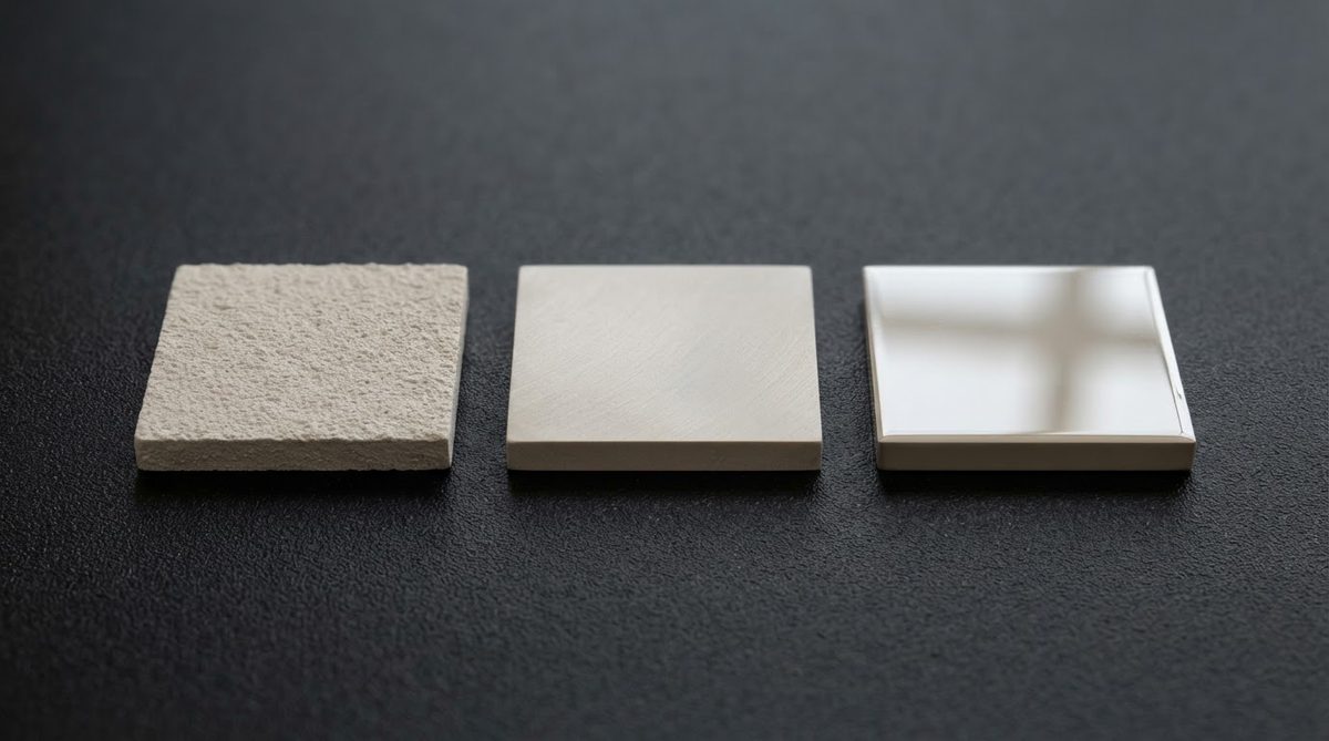
| Finish | Ra (µm) | Rz (µm) | Typical Method | Source |
|---|---|---|---|---|
| As-fired | 0.4–1.0 | 2.5–6.0 | Tape-cast or dry-pressed, sintered at 1,580–1,650 °C | CoorsTek ADS-96R datasheet |
| Lapped (one side) | 0.15–0.40 | 1.0–2.5 | Fixed-abrasive or free-abrasive flat lapping, SiC or diamond slurry | Kyocera A-493 datasheet |
| Polished (one side) | 0.02–0.05 | 0.1–0.3 | Multi-stage CMP with colloidal silica | Maruwa HA-96 datasheet |
Typical values for commercially available material, for comparison only. Confirm against the datasheet for your specific grade.
Ra (arithmetic average roughness) is the most commonly specified parameter, but Rz (average peak-to-valley height over five sampling lengths) often matters more for metallization adhesion. A substrate with the same Ra can have very different peak distributions, so request Rz or Rmax if your process is sensitive to outlier peaks.
How Alumina 96% Al2O3 Surface Roughness Affects Metallization and Bonding
Thick-Film Printing
Screen-printed thick-film conductors (Ag, AgPd, Au) rely on mechanical interlocking with the substrate surface during firing. Ra values of 0.3–0.8 µm typically give the best adhesion, measured per ASTM F1842 pull testing. Over-polishing a substrate before thick-film printing can actually reduce peel strength by 20–40%, because the paste has fewer anchor points.
Thin-Film Sputtering and DPC
Thin-film processes—sputtered Ti/Cu, Ti/Pt/Au, or AlN thin-film metallization—require smoother surfaces. Ra above 0.25 µm causes shadowing during sputter deposition, leading to voids at grain boundaries and reduced adhesion. For DPC (Direct Plated Copper) on 96% alumina, a lapped surface of Ra 0.15–0.25 µm is the practical minimum. Thin-film circuits with line widths below 50 µm typically need polished substrates at Ra ≤ 0.05 µm to maintain line-edge definition.
Wire Bonding
Gold ball bonding on thick-film gold pads is less sensitive to substrate roughness because the pad itself is 8–15 µm thick. Aluminum wedge bonding on thin-film pads is more demanding. For wedge bonds at 25 µm pitch, bond-pad roughness below Ra 0.1 µm is standard practice per JEDEC JESD22-B116. The substrate finish directly sets the pad roughness when the metallization layer is thin (< 2 µm).
Worked Example: Choosing a Finish for a Hybrid Module
Suppose you are designing a thick-film hybrid on a 50.8 × 50.8 mm 96% alumina substrate, 0.635 mm thick. The circuit uses screen-printed AgPd conductors (12 µm fired thickness) and gold wire bonds at 100 µm pitch.
- Metallization: Thick-film AgPd fires well on as-fired substrates. Ra 0.4–0.8 µm is acceptable.
- Wire bonding: At 100 µm pitch with 25 µm gold wire, the bond pad is thick enough (12 µm) that substrate roughness is not the limiting factor.
- Conclusion: As-fired finish is sufficient. Lapping would add 15–30% to substrate cost with no functional benefit.
Now change the scenario: the same substrate carries sputtered Ti/Cu traces at 30 µm line/space for a DPC circuit. Here, the alumina 96% Al2O3 surface roughness must drop below Ra 0.25 µm, so lapping is mandatory. If thin-film gold pads carry 20 µm-pitch wedge bonds, polishing to Ra ≤ 0.05 µm is the right call despite the cost premium.
How 96% Alumina Roughness Compares to Higher-Purity Grades
99.6% alumina substrates fire to a finer grain size (1–3 µm versus 3–8 µm for 96%) because the reduced glass-phase content allows tighter sintering. This gives polished 99.6% alumina a lower achievable Ra—down to 0.01 µm—compared to 0.02–0.05 µm for polished 96%. If your thin-film process demands sub-0.02 µm roughness, 96% alumina may not reach it even with extended CMP, and 99.6% Al2O3 substrates become the better choice.
Surface Finish Cost Comparison for 96% Al2O3
Finishing adds significant cost to raw substrates. The table below gives approximate multipliers relative to as-fired unit pricing for 96% alumina in moderate volumes (100–500 pieces).
| Finish | Cost Multiplier vs. As-Fired | Lead-Time Impact |
|---|---|---|
| As-fired | 1.0× | Baseline |
| Lapped (one side) | 1.15–1.30× | +2–5 days |
| Lapped (both sides) | 1.25–1.45× | +3–7 days |
| Polished (one side) | 1.40–1.80× | +5–10 days |
Enter your substrate size, finish level, and quantity below to estimate the cost difference between alumina 96% Al2O3 surface roughness options for 96% alumina substrates at volume.
[pcb_calc type=”finish-cost”]
When NOT to Specify a Smoother Finish
Over-specifying surface roughness wastes money and can hurt performance. Avoid lapping or polishing when:
- Thick-film only circuits: As-fired Ra 0.4–0.8 µm gives better paste adhesion than a polished surface.
- Structural or insulating substrates: If the alumina serves as a heatsink spacer or insulator with no metallization, surface roughness is cosmetic.
- High-volume consumer products: The cost delta of lapping at 10,000+ units can exceed the cost of the substrate itself. Evaluate whether an MCPCB or FR-4 with thermal vias meets the thermal requirement at lower total cost.
- Solder-reflow only assembly: Solder wetting depends on pad metallization, not substrate roughness. An as-fired substrate with properly fired thick-film pads solders identically to a polished one.
Measuring and Specifying Roughness on Your Drawing
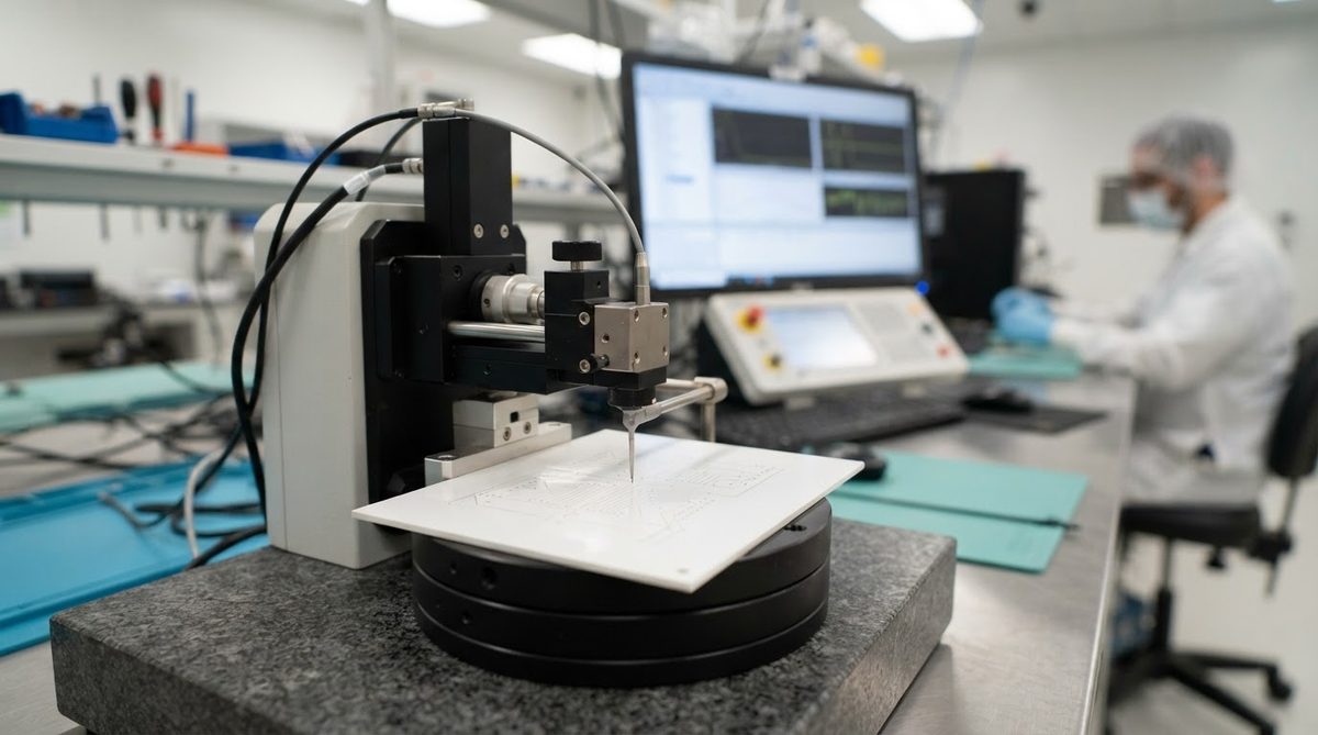
Specify alumina 96% Al2O3 surface roughness on your substrate drawing using ISO 4287 or ASME B46.1 notation. Include:
- Parameter: Ra is standard; add Rz if you need peak control.
- Value and tolerance: e.g., Ra ≤ 0.25 µm.
- Measurement length: A 4 mm evaluation length with 0.8 mm cutoff wavelength is typical for ceramic substrates per ISO 4288.
- Side: Specify which side (or both) requires the finish. Single-side lapping is cheaper and sufficient when only one face carries metallization.
Avoid specifying Ra alone without a cutoff wavelength. A 96% alumina surface measured at λc = 0.25 mm will report a lower Ra than the same surface measured at λc = 0.8 mm, because the shorter cutoff filters out longer-wavelength waviness. This is a common source of vendor–customer disputes.
FAQ
Can I get 96% alumina polished below Ra 0.02 µm?
It is difficult and not guaranteed. The 3–8 µm grain size of 96% alumina limits the achievable polish. Most suppliers quote Ra 0.02–0.05 µm as the practical floor. For sub-0.02 µm, switch to 99.6% alumina polished substrates with their finer grain structure.
Does lapping change the substrate thickness tolerance?
Yes, lapping improves thickness tolerance. As-fired 96% alumina is typically ±1–2% of nominal thickness. Lapping tightens this to ±0.5–1%, which matters for controlled-impedance RF circuits and tight assembly stacks.
Should I specify roughness on both sides of the substrate?
Only if both sides carry metallization or bonding. Single-side lapping costs 10–15% less than double-side and is the default for most single-layer circuits. The unfinished side retains the as-fired texture, which actually improves adhesive bond strength if the substrate is mounted to a heatsink.
How does alumina 96% Al2O3 surface roughness compare to AlN?
As-fired aluminum nitride (AlN) typically measures Ra 0.3–0.8 µm, similar to 96% alumina. Polished AlN reaches Ra 0.02–0.05 µm. The main difference is that AlN’s higher thermal conductivity (170–200 W/mK) makes it the better choice for high-power applications regardless of surface finish. See the full comparison in the AlN surface roughness guide.
What profilometer settings should I use to verify incoming substrates?
Use a stylus profilometer with a 2 µm tip radius, 0.8 mm cutoff wavelength (λc), and 4 mm evaluation length per ISO 4288. Take at least three traces across the substrate and average the results. Optical (white-light interferometry) methods also work but may read 10–20% lower Ra on ceramic surfaces due to different interaction with grain-boundary pores.