Alumina 96% Al2O3 laser machining is the most practical way to cut, scribe, and drill 96% alumina substrates when you need kerf widths under 100 µm, L/S features that diamond saws cannot reach, or rapid prototyping without hard tooling. CO2 lasers (9.4–10.6 µm) handle through-cuts up to about 1.0 mm thick; UV lasers (355 nm Nd:YAG or excimer) deliver finer features with a smaller heat-affected zone (HAZ) but at slower feed rates. This article covers parameter selection, achievable tolerances, surface effects, and the cases where alumina 96% Al2O3 laser machining is the wrong tool.
Why Alumina 96% Al2O3 Laser Machining Works Well
96% alumina is hard (Vickers hardness ~1400 HV per CoorsTek ADS-96R datasheet) and brittle. Mechanical routing wears tooling fast and risks edge chipping. Laser machining is a non-contact process: no tool wear, no clamping stress, no coolant contamination. It also allows complex 2-D profiles, slots, and arrays that would require multiple mechanical setups.
Alumina absorbs well in the mid-IR range, which is why CO2 lasers at 10.6 µm couple efficiently into the material. At UV wavelengths the absorption mechanism shifts toward photo-ablation, breaking Al–O bonds directly and producing cleaner edges. Both approaches work; the choice depends on feature size, throughput, and acceptable edge quality. If your project also needs laser-scribed snap lines on 96% alumina, the same CO2 source can handle both operations in a single setup.
CO2 vs. UV Laser for Alumina 96% Al2O3 Laser Machining
| Parameter | CO2 (10.6 µm) | UV Nd:YAG (355 nm) | Unit |
|---|---|---|---|
| Typical kerf width | 80–150 | 20–50 | µm |
| Positional accuracy | ±25–50 | ±5–15 | µm |
| HAZ depth (96% Al2O3, 0.635 mm) | 30–80 | 5–15 | µm |
| Max practical through-cut thickness | ~1.0 | ~0.38 | mm |
| Relative throughput (full-cut, same geometry) | 1× | 0.2–0.4× | — |
| Relative cost per part (volume) | Lower | Higher | — |
Typical values for commercially available 96% alumina substrates. Confirm against the datasheet for your specific grade.
For most substrate singulation and basic via drilling, CO2 is the workhorse. Choose UV when you need edge roughness below Ra 1.0 µm, features smaller than 80 µm, or minimal recast on a surface that will carry thin-film metallisation. Comparing alumina grades, laser machining of AlN substrates requires different wavelength coupling considerations because AlN’s thermal conductivity is 6–8× higher than 96% alumina, pulling heat away from the cut zone faster.
Key Process Parameters and Their Effects
Power and pulse frequency
Higher average power increases material removal rate but widens the HAZ. For alumina 96% Al2O3 laser machining on a 0.635 mm thick substrate with a 50 W CO2 laser, a typical starting point is 30–40 W average power at 5–20 kHz pulse frequency, with multiple passes at 50–150 mm/s scan speed. Reducing power and increasing pass count keeps the HAZ narrow at the cost of cycle time.
Focus and beam quality
A tightly focused beam (spot diameter 50–80 µm for CO2, 15–25 µm for UV) gives the narrowest kerf. Defocusing even 0.1 mm widens the cut and increases taper. On substrates thicker than 0.5 mm, the taper angle through a CO2 cut can reach 3–5°, which matters if the edge carries a ground plane or must mate flush with another part.
Assist gas
Nitrogen or compressed air blown coaxially clears debris and reduces recast deposition. Oxygen assist is sometimes used to increase removal rate, but it can oxidise exposed metallisation on already-patterned substrates. For bare substrates, nitrogen at 2–4 bar is the safe default.
Enter your substrate thickness, laser type, and desired kerf width below to estimate pass count and cycle time for your alumina 96% Al2O3 laser machining job.
Worked Example: Through-Cut of a 0.635 mm Substrate
Suppose you need to singulate a 25 × 25 mm panel of 96% alumina (0.635 mm thick) into 5 × 5 mm individual substrates using a 50 W CO2 laser.
- Grid layout: 5 columns × 5 rows = 25 parts. Total cut length along X: 4 internal lines × 25 mm = 100 mm. Along Y: 4 × 25 mm = 100 mm. Perimeter: 4 × 25 mm = 100 mm. Total: 300 mm.
- Parameters: 35 W, 10 kHz, scan speed 100 mm/s, 3 passes per line.
- Cut time: 300 mm ÷ 100 mm/s = 3 s per pass × 3 passes = 9 s of lasing. Add ~50% for acceleration, deceleration, and repositioning → ~14 s total.
- Kerf width: ~100 µm. Material lost per cut line: 100 µm. Design your panel pitch at 5.0 mm + 0.10 mm = 5.10 mm centre-to-centre to account for kerf.
- HAZ: At these settings, expect 40–60 µm of micro-cracked or recast zone on each cut face. If the edge will be metallised or wire-bonded, add a 0.15 mm keep-out from the cut line.
Surface Quality After Alumina 96% Al2O3 Laser Machining
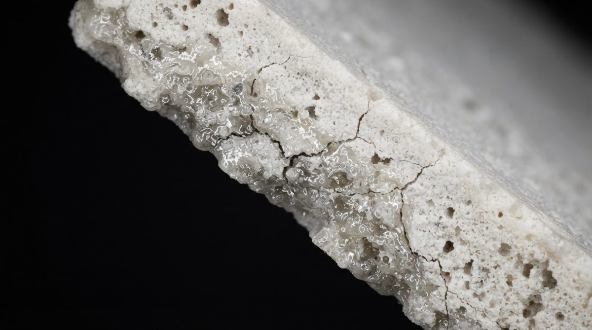
A CO2-cut edge on 96% alumina typically shows Ra 1.5–4.0 µm, with a thin recast layer of re-solidified alumina and glassy phase. UV-cut edges are smoother, often Ra 0.5–1.5 µm, with less recast. For context, the as-fired surface of 96% alumina is usually Ra 0.4–0.8 µm (per CoorsTek ADS-96R data). Laser-cut edges are therefore rougher than the substrate face. If your design demands tight surface control on cut faces, review the surface roughness specifications for 96% alumina and consider post-cut lapping.
Micro-cracks in the HAZ can reduce flexural strength locally. ASTM C1161 four-point bend testing on laser-cut 96% alumina coupons typically shows 10–20% lower strength compared to diamond-scribed or as-fired edges, depending on laser parameters. For structural substrates under mechanical load, this matters. For most electronic substrates clamped in a housing, it does not.
When NOT to Use Laser Machining on 96% Alumina
Thick substrates (>1.0 mm): CO2 laser through-cuts above 1.0 mm require many passes, produce excessive taper, and risk thermal shock cracking. Diamond sawing or waterjet is more practical.
High-volume simple rectangles: If you need 100k+ identical rectangular substrates with no internal features, diamond scribing and breaking is faster and cheaper per part.
Tight edge-strength requirements: Applications where the substrate is a structural element under bending load may not tolerate the HAZ-induced strength reduction. Mechanical grinding gives a stronger edge.
Very large panels: Laser machining a 150 × 150 mm outline is slow and expensive. Waterjet or CNC diamond routing handles large perimeters better.
If your project calls for higher purity and finer features, consider custom 99.6% alumina PCB fabrication, which offers tighter grain structure and smoother laser-cut edges.
Comparing Alumina Grades for Laser Machining
| Property | 96% Al2O3 | 99.6% Al2O3 | Unit / Condition | Source |
|---|---|---|---|---|
| Thermal conductivity | 24–28 | 30–35 | W/mK at 25 °C | CoorsTek ADS-96R / ADS-996 |
| Flexural strength | 340–380 | 380–450 | MPa (ASTM C1161) | CoorsTek |
| Grain size | 5–15 | 2–5 | µm | Kyocera A-493 / A-479 |
| Laser-cut edge Ra (CO2, 0.635 mm) | 1.5–4.0 | 1.0–2.5 | µm | Typical production data |
| Relative substrate cost | 1× | 1.8–2.5× | — | Market pricing |
Typical values for commercially available material, for comparison only. Confirm against the datasheet for your specific grade.
99.6% alumina’s finer grain structure produces smoother cut edges and a thinner HAZ. But the cost premium is significant. For most thick-film hybrid circuits and sensor substrates, alumina 96% Al2O3 laser machining delivers the right balance of machinability, performance, and price.
Frequently Asked Questions
Can I laser-drill vias in 96% alumina?
Yes. CO2 lasers can drill vias down to about 100 µm diameter in 0.635 mm substrates. UV lasers reach 30–50 µm. Aspect ratios above 3:1 become difficult because debris re-deposits inside the hole, so for deep vias in thick substrates, mechanical drilling or green-state punching is more reliable.
Does alumina 96% Al2O3 laser machining damage existing metallisation?
It can. If the laser beam crosses or approaches a metallised trace, reflected and conducted heat can delaminate or melt the conductor. Maintain a minimum 0.15 mm clearance between the cut path and any metal feature. For already-patterned substrates, program the cut path to avoid metal, or cut before metallisation.
What file format should I supply for laser machining?
DXF is the most universally accepted format for laser tool paths. Supply the cut geometry as closed polylines on a single layer, with the kerf compensation noted in your drawing. Gerber files work if the fab house converts them, but DXF avoids translation errors.
How does laser machining compare to waterjet for alumina?
Waterjet produces no HAZ and handles thick substrates well, but kerf width is 200–400 µm and positional accuracy is ±50–100 µm. Laser wins on precision and fine features; waterjet wins on thick sections and zero thermal impact.
Is there a minimum order for laser-machined alumina substrates?
Most ceramic PCB fabricators, including AluminaPCB, accept prototype quantities. Laser machining has no hard tooling, so there is no tooling cost to amortise. Single-piece orders are common for prototyping. For volume pricing, request a 96% alumina wholesale quote.
Next Step
If you have a substrate outline, via pattern, or panel layout ready, upload your DXF or Gerber to get a quote. For general questions about ceramic substrate types and which grade fits your application, the materials comparison page is a good starting point.