Alumina 96% Al2O3 custom PCBs offer 24–28 W/mK thermal conductivity, dielectric strength above 10 kV/mm, and continuous operating temperatures past 800 °C—all at roughly one-third the cost per unit area of aluminum nitride. That combination makes 96% alumina the default ceramic substrate for power electronics, LED thermal management, RF modules, and sensor assemblies where FR-4 cannot survive the thermal or frequency demands.
Key Takeaways
- 96% alumina provides 24–28 W/mK thermal conductivity at 20 °C (per CoorsTek ADS-96R datasheet), roughly 10× higher than FR-4.
- Dielectric constant sits at 9.0–9.5 at 1 MHz, stable up to several GHz, making it suitable for many RF and high-voltage isolation designs.
- Flexural strength of 340–380 MPa (ASTM C1161, 4-point bend) is adequate for most board-level assemblies but demands careful handling during pick-and-place.
- Standard fabrication routes include thick film, thin film (sputtered metallisation), DPC, and HTCC, each targeting different line/space and volume requirements.
- Where thermal conductivity above 100 W/mK is required, custom aluminum nitride PCB fabrication is the better path.
96% Alumina Substrate Properties at a Glance
| Parameter | Value | Unit | Condition | Source |
|---|---|---|---|---|
| Al₂O₃ purity | 96 ± 0.5 | % | — | CoorsTek ADS-96R |
| Thermal conductivity | 24–28 | W/mK | 20 °C | CoorsTek ADS-96R |
| CTE | 7.2–8.2 | ppm/°C | 25–400 °C | Kyocera A-493 |
| Dielectric constant (εr) | 9.0–9.5 | — | 1 MHz, 25 °C | CoorsTek ADS-96R |
| Dielectric strength | >10 | kV/mm | AC, 25 °C | Kyocera A-493 |
| Flexural strength | 340–380 | MPa | 4-pt bend, ASTM C1161 | CoorsTek ADS-96R |
| Volume resistivity | >1014 | Ω·cm | 25 °C | Kyocera A-493 |
| Max continuous use temp. | ~1 600 | °C | Unloaded, in air | CeramTec Rubalit 708S |
Typical values for commercially available material, for comparison only. Confirm against the datasheet for your specific grade.
Fabrication Processes for Custom 96% Alumina PCBs
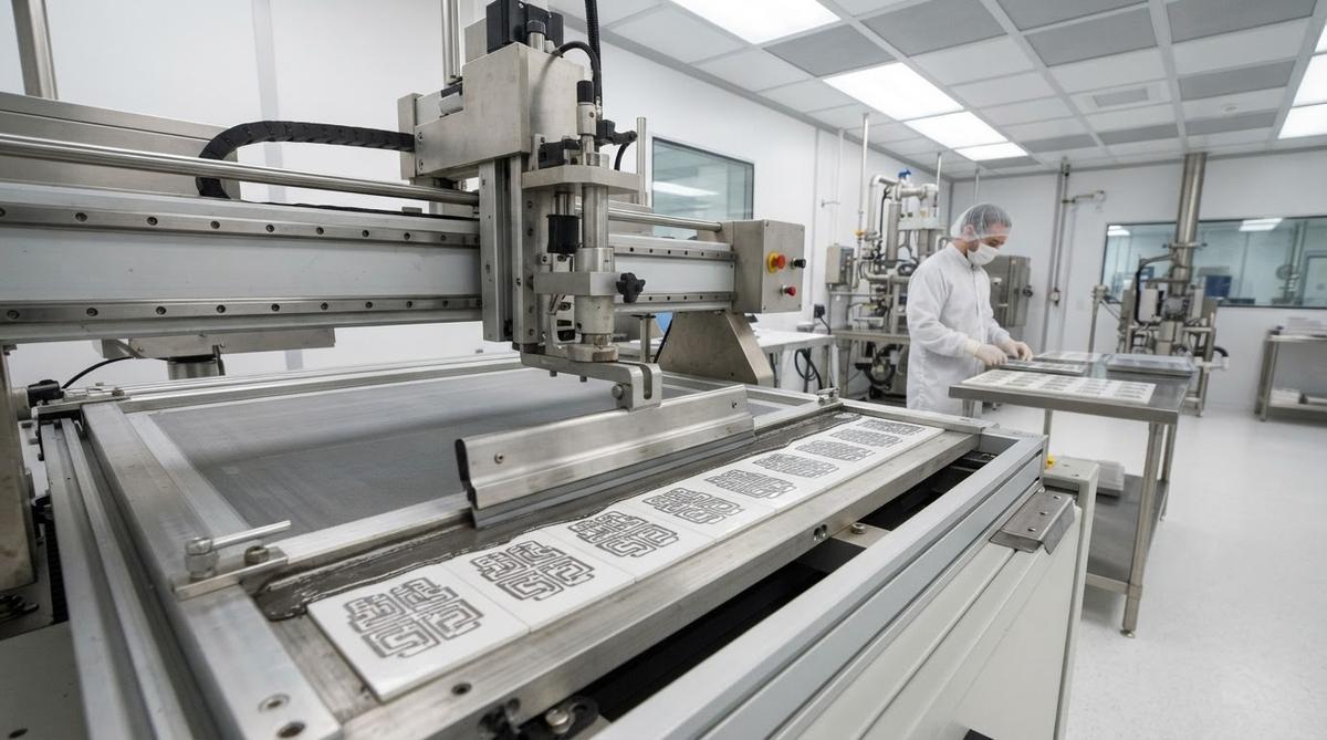
Thick Film
Screen-printed conductors (typically silver, gold, or palladium-silver pastes) are fired at 850–1 000 °C onto a pre-sintered alumina substrate. Line/space is generally limited to 100–125 µm, which is adequate for power routing and resistor networks. Thick film is the lowest-cost metallisation route and handles high volumes well.
Thin Film (Sputtered Metallisation)
Sputtered Ti/Ni/Au or Cr/Ni/Au stacks achieve line/space down to 20–30 µm. The process adds cost per unit area but enables tighter RF impedance control and finer pitch die attach pads. Thin film on 96% alumina is common in hybrid microelectronics and mmWave modules.
DPC (Direct Plated Copper)
A sputtered seed layer followed by electroplated copper yields copper thickness from a few micrometres up to ~100 µm. DPC combines fine-line capability (≈30–50 µm line/space) with good current-carrying capacity. It suits mid-power LED arrays and sensor substrates. For a deeper look at alumina 96% dielectric properties for PCB design, see the dedicated page.
HTCC (High-Temperature Co-fired Ceramic)
Green alumina tape is printed with tungsten or molybdenum paste, stacked, and co-fired above 1 500 °C. HTCC produces monolithic multilayer packages with hermetic via interconnects. It is the standard for military and aerospace hermetic housings. The trade-off: tungsten and moly have higher resistivity than copper or silver, so HTCC is not ideal for low-loss RF signal lines.
Design Considerations Specific to 96% Alumina
CTE Matching
96% alumina’s CTE of 7.2–8.2 ppm/°C sits between silicon (~2.6 ppm/°C) and copper (~17 ppm/°C). For bare-die attach, a compliant solder (e.g., SAC305 or AuSn for high reliability) absorbs the mismatch over small die sizes. For die larger than about 10 × 10 mm, consider a CTE-matched heat spreader or move to custom silicon nitride PCBs for their superior fracture toughness under thermal cycling.
Mechanical Handling
Ceramic is brittle. Design generous edge clearances (≥0.5 mm from conductor to substrate edge) and specify chamfered or laser-rounded corners where possible. Panels with laser-scribed snap lines singulate cleanly without introducing micro-cracks.
Surface Finish
Substrate surface roughness affects both metallisation adhesion and wire-bond pull strength. As-fired alumina typically runs Ra 0.4–0.8 µm. If your design needs finer lines or stronger thin-film adhesion, specify a polished or lapped alumina 96% substrate with Ra < 0.1 µm.
Worked Example: Thermal Resistance of a 96% Alumina Substrate
Suppose you need to spread 5 W from a 3 × 3 mm LED die through a 0.635 mm thick alumina substrate.
- Substrate area under the die: 9 mm² = 9 × 10⁻⁶ m².
- Thermal conductivity (k): 25 W/mK (mid-range for 96% alumina at 20 °C).
- Thickness (t): 0.635 mm = 6.35 × 10⁻⁴ m.
- Conduction thermal resistance: Rth = t / (k × A) = 6.35 × 10⁻⁴ / (25 × 9 × 10⁻⁶) = 2.82 °C/W.
- Temperature rise across the substrate: ΔT = 5 W × 2.82 °C/W ≈ 14.1 °C.
This is a 1-D approximation. Real spreading resistance is lower because heat fans out laterally. Still, 14 °C across the substrate is manageable for most LED designs. If your calculation shows ΔT above 25–30 °C, consider a thinner substrate (0.38 mm) or a higher-conductivity material like AlN.
96% Alumina vs. 99.6% Alumina: When to Upgrade
| Parameter | 96% Al₂O₃ | 99.6% Al₂O₃ | Unit / Condition |
|---|---|---|---|
| Thermal conductivity | 24–28 | 30–35 | W/mK, 20 °C |
| Dielectric constant | 9.0–9.5 | 9.7–9.9 | 1 MHz |
| Flexural strength | 340–380 | 380–450 | MPa, ASTM C1161 |
| Surface finish (as-fired Ra) | 0.4–0.8 | 0.3–0.5 | µm |
| Relative substrate cost | 1× | 1.5–2× | — |
Typical values for commercially available material, for comparison only. Confirm against the datasheet for your specific grade.
For most power and LED applications, 96% alumina is sufficient. Upgrade to custom 99.6% alumina PCB fabrication when you need tighter thin-film line/space on a smoother surface, higher hermeticity, or the incremental thermal gain matters in your stack-up.
When Not to Use 96% Alumina
High thermal flux above ~50 W/cm²: AlN at 170–200 W/mK handles dense power stages far better. The substrate cost premium pays for itself in smaller heat sinks.
Large-area boards with complex routing: If your design exceeds roughly 150 × 150 mm with more than four layers of signal routing, FR-4 or metal-core PCB is cheaper and mechanically easier to handle.
Severe thermal cycling with large die: Silicon nitride (Si₃N₄) offers 3–4× the fracture toughness of alumina and survives aggressive –55 °C to +175 °C cycling far longer.
Low-frequency, low-power consumer electronics: Standard FR-4 at $0.02–0.05/cm² beats alumina at $0.30–1.00/cm² when thermal and dielectric requirements are modest.
Frequently Asked Questions
What is the maximum operating temperature of a 96% alumina PCB?
The bare alumina substrate can withstand over 1 600 °C in air. The practical limit is set by the metallisation: thick-film silver/gold conductors are stable to about 300–400 °C continuous, while tungsten HTCC metallisation operates above 500 °C. Always derate for the weakest link in your assembly—solder, epoxy, or wire bond.
Can I solder standard SMD components onto a 96% alumina PCB?
Yes. Standard SAC305 reflow profiles work on alumina substrates with thick-film or DPC metallisation. Use a slow ramp rate (1–2 °C/s) to avoid thermal shock to the ceramic. Preheat to at least 150 °C before peak reflow.
How does 96% alumina compare to aluminum nitride for LED substrates?
For LEDs dissipating under ~3 W per device, 96% alumina provides adequate thermal performance at one-third to one-fifth the substrate cost of AlN. Above 5–10 W per device, AlN’s 170–200 W/mK conductivity meaningfully reduces junction temperature and extends LED lifetime.
What minimum line/space can I achieve on 96% alumina?
Thick film: 100–125 µm line/space. DPC: 30–50 µm. Thin film (sputtered): 20–30 µm. The choice depends on your circuit density and budget. Thin film adds significant per-unit cost but enables RF-grade impedance control.
Is 96% alumina suitable for RF and microwave circuits?
It works well up to about 10–20 GHz for many hybrid designs. The εr of 9.0–9.5 is stable with temperature and frequency, and loss tangent is low (0.0001–0.0004 at 1 MHz per CoorsTek data). Above 40 GHz, lower-εr substrates like quartz or certain LTCC systems may offer better impedance matching.
Next Step
If your thermal and dielectric requirements fit the 96% alumina envelope, prepare your Gerber files and substrate dimensions. For volume pricing on custom alumina boards, or to discuss metallisation options with an engineer, request a quote directly.