A silicon nitride Si3N4 custom PCB is the toughest ceramic substrate option available for power electronics fabrication, with a fracture toughness of 6–7 MPa·√m — roughly three to four times that of aluminum nitride and six times that of 96% alumina. That mechanical advantage makes silicon nitride Si3N4 custom PCB assemblies the preferred choice for power modules, EV inverters, and other designs that endure deep thermal cycling. Custom fabrication is possible, but the material demands specific metallization processes and tighter design awareness than alumina or AlN.
Key Takeaways
- Si3N4 fracture toughness of 6–7 MPa·√m (per ASTM C1421) far exceeds AlN (~3 MPa·√m) and Al2O3 96% (~3.5 MPa·√m), reducing cracking under thermal shock.
- Thermal conductivity ranges from 25–90 W/mK depending on grade; high-purity sintered grades from Toshiba and Kyocera reach 80–90 W/mK.
- Active Metal Brazing (AMB) is the primary metallization method for silicon nitride Si3N4 custom PCB substrates; DBC is technically possible but rarely used because the bonding temperature risks degrading the ceramic.
- Si3N4 substrates cost roughly 5–10× more than equivalent Al2O3 96% and 2–4× more than AlN, so the material is justified only when thermal-cycling reliability is the dominant requirement.
- Standard substrate thicknesses for custom Si3N4 PCBs are 0.25 mm, 0.32 mm, and 0.635 mm.
What Makes a Silicon Nitride Si3N4 Custom PCB Different from Other Ceramic Substrates
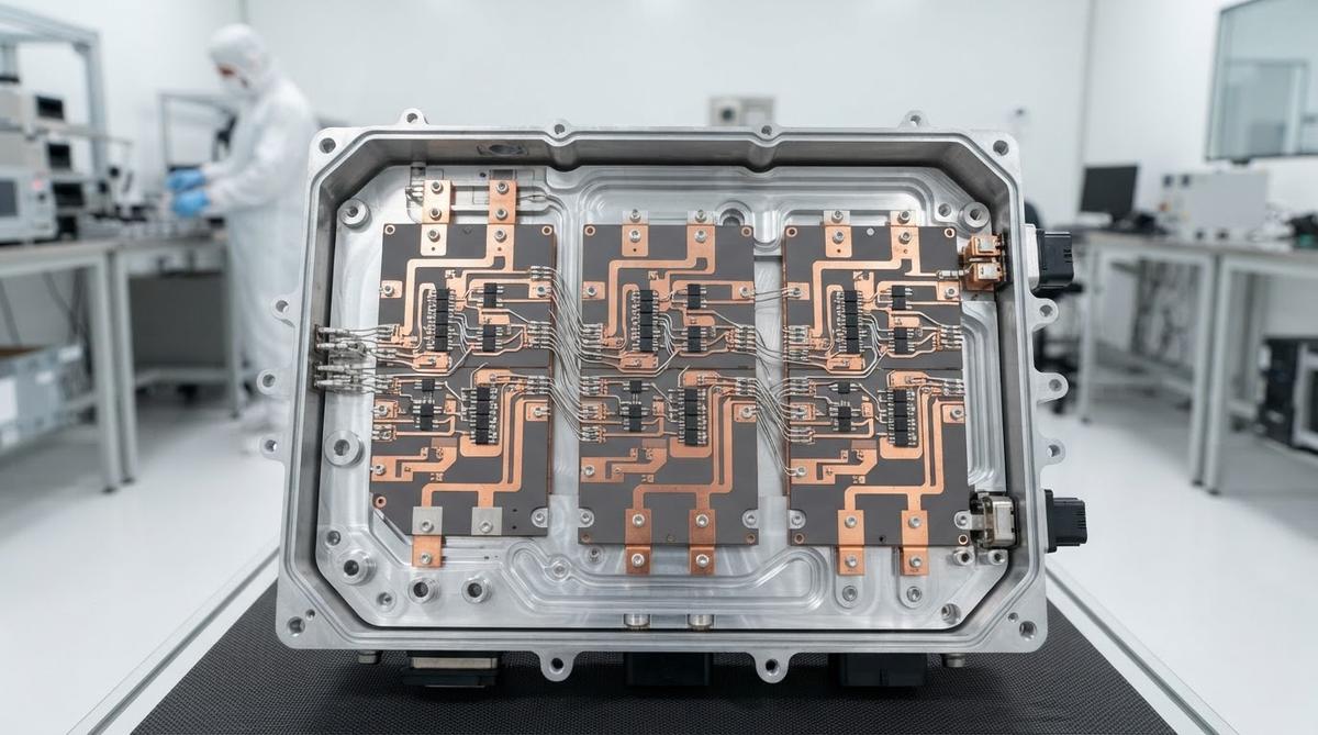
The defining property of silicon nitride is its combination of high flexural strength (600–900 MPa per ASTM C1161) and fracture toughness. Where alumina and aluminum nitride are strong in compression but brittle under tensile or bending loads, Si3N4 resists crack propagation far more effectively. This is critical in power electronics, where repeated heating and cooling cycles generate thermomechanical stress at the solder and substrate interfaces.
The trade-off is thermal conductivity. Standard-grade Si3N4 conducts heat at only 25–30 W/mK — comparable to 96% alumina and far below AlN’s 170–200 W/mK. High-thermal-conductivity (HTC) grades, such as Toshiba’s SN-HTC, push this to 80–90 W/mK, but at a significant cost premium. For a deeper look at these values, see the Si3N4 material properties datasheet.
Si3N4 Compared to Al2O3 and AlN Substrates
| Parameter | Al2O3 96% | AlN | Si3N4 (HTC grade) | Unit | Condition / Source |
|---|---|---|---|---|---|
| Thermal conductivity | 24–28 | 170–200 | 80–90 | W/mK | 20 °C; Kyocera / Toshiba datasheets |
| Flexural strength | 300–380 | 300–350 | 600–900 | MPa | ASTM C1161, 3-pt bend |
| Fracture toughness | 3.3–3.7 | 2.6–3.2 | 6–7 | MPa·√m | ASTM C1421 |
| CTE (25–400 °C) | 7.2–7.8 | 4.5–5.0 | 2.7–3.2 | ppm/K | Kyocera / CoorsTek datasheets |
| Dielectric strength | 10–15 | 14–17 | 12–18 | kV/mm | IEC 60243 |
| Relative cost (per cm²) | 1× | 3–5× | 5–10× | — | Industry estimate, 2024 |
Typical values for commercially available material, for comparison only. Confirm against the datasheet for your specific grade.
Si3N4’s low CTE (2.7–3.2 ppm/K) is closer to silicon (2.6 ppm/K) than either alumina or AlN. This reduces stress at the die-attach interface during thermal cycling, which is one reason silicon nitride Si3N4 custom PCB substrates dominate in SiC and GaN power modules where junction temperatures regularly exceed 200 °C. For a broader comparison of substrate ceramics, see our guide to ceramic PCB materials compared.
Fabrication Processes for Silicon Nitride Si3N4 Custom PCB Production
Active Metal Brazing (AMB)
AMB is the standard metallization route for Si3N4. A braze alloy containing an active element — typically titanium in an AgCuTi system — wets the nitride surface at 800–900 °C in a vacuum furnace. The result is a direct chemical bond between copper foil and the ceramic. AMB produces copper layers from 0.3 mm to 0.8 mm thick, which carry high currents and spread heat effectively.
AMB on Si3N4 survives thermal-cycling tests that destroy DBC-on-AlN. Published data from Infineon and others show AMB-Si3N4 substrates passing >3,000 cycles at ΔT = 200 °C (–40 °C to +175 °C) without delamination, compared to typical DBC-AlN failure at 500–1,000 cycles under the same conditions.
Why Not DBC or Thick Film?
Direct Bonded Copper (DBC) requires oxidizing the ceramic surface to form a copper-oxide eutectic at ~1,065 °C. Si3N4 does not oxidize as readily as Al2O3 or AlN, and the high bonding temperature can degrade the grain-boundary phase that gives Si3N4 its toughness. Some manufacturers offer DBC-Si3N4, but adhesion strength and reliability are inferior to AMB. Thick-film and thin-film metallization are used for resistor networks and fine traces on alumina, but they are not standard on Si3N4 substrates.
Laser Scribing and Machining
Si3N4 is harder to machine than alumina. Diamond scribing works but wears tooling quickly. Laser scribing (typically Nd:YAG or CO2) is preferred for singulation and via formation. If your design requires laser-scribed Si3N4 substrates, specify the kerf width and heat-affected zone tolerance early — laser parameters affect edge strength.
Enter your substrate material, thickness, and operating temperature below to see how thermal performance derates across the range relevant to your silicon nitride Si3N4 custom PCB design.
Design Rules for Custom Si3N4 Circuit Boards
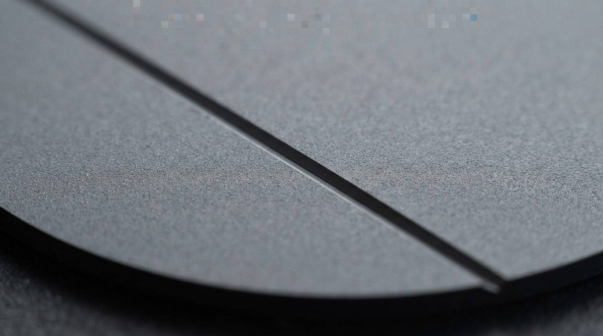
Most custom Si3N4 boards are single- or double-sided power substrates, not multilayer signal boards. Keep these constraints in mind:
- Substrate thickness: 0.25 mm, 0.32 mm, or 0.635 mm are standard. Thinner substrates reduce thermal resistance but are harder to handle. For ultra-thin options, see thin Si3N4 substrates.
- Copper thickness: 0.3 mm is typical for AMB; 0.5–0.8 mm is available for high-current paths.
- Minimum trace/gap: AMB typically achieves 0.3–0.5 mm trace/space, far coarser than DPC on alumina. Design accordingly.
- Panel size: Standard Si3N4 blanks from major suppliers (Toshiba, Kyocera, Maruwa) are available up to ~190 mm × 140 mm. Larger panels are possible but drive cost up sharply.
- Edge clearance: Keep copper patterns at least 0.5 mm from the substrate edge to avoid stress concentration and partial delamination during brazing.
Worked Example: Thermal Resistance of a Si3N4 Power Substrate
Consider a 40 mm × 40 mm Si3N4 substrate, 0.32 mm thick, HTC grade (k = 85 W/mK). The conduction thermal resistance through the ceramic alone is:
Rth = t / (k × A) = 0.00032 / (85 × 0.0016) = 0.0024 °C/W
For a 200 W SiC MOSFET die mounted on this substrate, the temperature drop across the ceramic is only ~0.47 °C. The ceramic layer itself is rarely the thermal bottleneck — solder joints and copper-to-heatsink interfaces dominate total Rth. The reason you pick a silicon nitride Si3N4 custom PCB is not raw conductivity; it is survival under thousands of thermal cycles.
When NOT to Use Si3N4
Si3N4 is overkill — and overpriced — for many applications. Choose a different substrate if:
- Thermal cycling is mild (ΔT < 100 °C, < 500 cycles): AlN with DBC is cheaper and thermally superior.
- You need fine-pitch traces (< 0.2 mm): DPC on alumina or AlN handles much finer features.
- Your budget is fixed and volumes are high: Al2O3 96% costs a fraction of Si3N4. If the mechanical environment is benign, alumina works fine.
- You need multilayer routing: LTCC on alumina or HTCC is the correct path. Si3N4 is not processed via LTCC or HTCC.
- RF or high-frequency signal integrity is the priority: AlN or low-loss alumina grades have better-characterized dielectric properties at GHz frequencies.
Frequently Asked Questions
Can Si3N4 substrates handle lead-free soldering temperatures?
Yes. Si3N4 withstands peak reflow temperatures well above 260 °C without damage. The ceramic itself is stable to over 1,000 °C in air. The limiting factor is the braze joint and copper adhesion, both of which tolerate standard lead-free profiles with margin.
What is the typical lead time for a silicon nitride Si3N4 custom PCB?
Expect 4–8 weeks for prototypes, depending on substrate sourcing and AMB processing. Si3N4 blanks are not stocked as widely as alumina, so substrate availability often sets the schedule. Ordering Si3N4 substrates in wholesale quantities can reduce lead time on repeat orders.
Is Si3N4 suitable for wire bonding?
Yes, provided the copper surface is plated with a bondable finish — typically Ni/Au (electroless nickel / immersion gold) or Ni/Ag. Aluminum wedge bonding and gold ball bonding are both used on Si3N4 power modules. Surface roughness of the plated copper should be specified to the bonder’s requirements.
Does Si3N4 outgas in vacuum or space environments?
Sintered Si3N4 has very low outgassing. Published NASA ASTM E595 test data on Si3N4 ceramics show TML (total mass loss) below 0.1% and CVCM (collected volatile condensable material) below 0.01%, meeting typical spacecraft material requirements.
How does Si3N4-AMB compare to AlN-DBC on cost per thermal cycle?
Si3N4-AMB costs more per unit but survives 3–10× more thermal cycles than AlN-DBC. For applications requiring >1,000 power cycles at ΔT ≥ 150 °C, the lifetime cost per cycle is often lower with Si3N4 because you avoid field failures and warranty replacements.
Next Step
If your power module or EV inverter design demands substrate survival beyond 1,000 deep thermal cycles, Si3N4-AMB is the substrate to evaluate. Download the Si3N4 substrate datasheet for full mechanical and thermal specifications, or request a quote for your custom layout.