An alumina 99.6% Al2O3 custom PCB uses a high-purity ceramic substrate with thermal conductivity of 28–35 W/m·K at 25 °C, dielectric constant of 9.7–9.9 at 1 MHz, and flexural strength of 350–400 MPa (per ASTM C1161). Compared to the widely used 96% grade, the 99.6% grade offers roughly 20–30% better thermal performance and measurably lower dielectric loss, making it the standard choice for RF power amplifiers, high-reliability sensor packages, and laser submounts where every fraction of a dB or degree matters.
Key Takeaways
- 99.6% Al2O3 conducts heat at 28–35 W/m·K versus 24–28 W/m·K for 96% alumina, both at 25 °C (source: CoorsTek ADS-996 datasheet).
- Dielectric loss tangent drops to 0.0001–0.0002 at 1 MHz, roughly half that of 96% alumina, which directly improves Q-factor in RF circuits.
- The material costs 1.5–2.5× more per unit area than 96% alumina; machining is also harder due to higher hardness (≈15.2 GPa Vickers).
- Compatible fabrication processes include thin-film metallization, thick-film screen printing, and DPC (Direct Plated Copper). HTCC and LTCC are also used with appropriate formulations.
- Typical applications: millimeter-wave modules, hermetic packages, high-power LED submounts, and medical implant electronics.
99.6% vs. 96% Alumina: Property Comparison
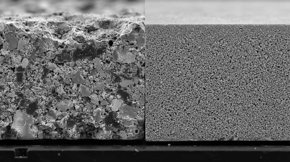
The 3.6-percentage-point difference in purity has a disproportionate effect on several properties. The additional alumina content replaces glassy-phase sintering aids (typically SiO2, MgO, CaO) that dominate grain boundaries in 96% grades. Fewer grain-boundary phases mean lower dielectric loss, higher thermal conductivity, and better hermeticity.
| Parameter | 96% Al2O3 | 99.6% Al2O3 | Unit | Condition | Source |
|---|---|---|---|---|---|
| Thermal conductivity | 24–28 | 28–35 | W/m·K | 25 °C | CoorsTek ADS-996 / Kyocera A-493 |
| Dielectric constant (εr) | 9.4–9.6 | 9.7–9.9 | — | 1 MHz | CoorsTek / Maruwa HA-996 |
| Loss tangent (tan δ) | 0.0002–0.0004 | 0.0001–0.0002 | — | 1 MHz | CoorsTek ADS-996 |
| Flexural strength | 330–380 | 350–400 | MPa | ASTM C1161, 4-pt bend | CoorsTek / CeramTec |
| Vickers hardness | 12–14 | 14.5–15.5 | GPa | HV 1 kg | Kyocera A-493 |
| CTE | 7.2–8.0 | 7.1–7.8 | ppm/°C | 25–300 °C | CoorsTek / Maruwa |
| Volume resistivity | >1014 | >1014 | Ω·cm | 25 °C | CoorsTek |
| Water absorption | 0.0 | 0.0 | % | — | Both grades fully dense |
Typical values for commercially available material, for comparison only. Confirm against the datasheet for your specific grade.
For a deeper look at how purity affects electrical behavior, see dielectric properties of ceramic substrates. If your thermal load is moderate and cost is the primary driver, standard 96% alumina PCB fabrication may be the better fit.
When to Specify 99.6% Al2O3 Over 96%
The upgrade is justified in a handful of specific scenarios. If none of these apply, 96% alumina will serve you well at lower cost.
- RF and microwave circuits above 10 GHz. The halved loss tangent translates to measurably lower insertion loss in transmission lines and filters. At 77 GHz automotive radar frequencies, the difference can be 0.1–0.2 dB/cm.
- Hermetic packaging. The near-zero glassy phase improves hermeticity and reduces outgassing, critical for sealed sensor cavities and military-grade hybrid modules per MIL-STD-883.
- Thin-film metallization. Sputtered Ti/Pt/Au or TaN resistor films adhere more uniformly to the finer grain structure of 99.6% substrates. Surface roughness after lapping can reach Ra < 0.05 µm. For substrates prepared this way, see polished 99.6% alumina substrates.
- High-temperature operation. Devices operating continuously above 300 °C benefit from the absence of low-melting-point grain-boundary glasses that can soften or degrade in 96% grades.
Fabrication Processes for 99.6% Al2O3 Custom PCBs
The higher hardness and finer microstructure of 99.6% alumina affect every downstream fabrication step. Here is what to expect.
Substrate Preparation
Blanks are typically supplied as-fired with surface roughness Ra 0.4–0.8 µm. For thin-film circuits, lapping and polishing bring Ra below 0.1 µm. Laser scribing creates snap lines for panelization; the harder material requires slightly higher laser energy than 96% substrates. Details on scribing options are covered at laser-scribed 99.6% alumina substrates.
Metallization Options
Thin-film (sputtered/evaporated): Ti/Pt/Au, Cr/Ni/Au, TaN resistor layers. Line/space down to 10–25 µm. Best for RF, MEMS, and precision resistor networks.
Thick-film (screen-printed): Ag, AgPd, Au, or Cu pastes fired at 850–950 °C. Line/space typically 100–150 µm. Lower cost per circuit, suitable for power hybrids and sensor substrates.
DPC (Direct Plated Copper): Sputtered seed layer followed by electroplated copper, 10–100 µm thick. Combines fine-line capability (≈30 µm line/space) with high current-carrying capacity. Good for LED thermal substrates and power modules.
Worked Example: Thermal Resistance of a 99.6% Al2O3 Submount
Consider a GaN HEMT die (3 mm × 3 mm) dissipating 10 W, mounted on a 99.6% alumina substrate 0.381 mm (15 mil) thick.
Conduction thermal resistance through the substrate:
Rth = t / (k × A) = 0.000381 m / (32 W/m·K × 9 × 10⁻⁶ m²) = 1.32 °C/W
With a 96% alumina substrate at 26 W/m·K, the same geometry gives 1.63 °C/W. The 99.6% grade saves 0.31 °C/W, which at 10 W means a 3.1 °C lower junction temperature. In a multi-stage amplifier with four such devices, that is 12.4 °C of cumulative thermal headroom. If your thermal budget is tighter still, custom aluminum nitride (AlN) PCBs offer 170–200 W/m·K but at substantially higher cost.
Design Rules and Tolerances
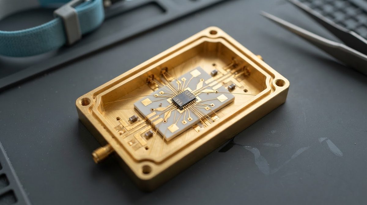
These are representative values. Confirm with your fabrication partner for your specific metallization process and substrate thickness.
| Parameter | Thin-Film | Thick-Film | DPC |
|---|---|---|---|
| Min. line / space | 10–25 µm | 100–150 µm | 25–50 µm |
| Conductor thickness | 0.5–5 µm | 8–15 µm (fired) | 10–100 µm |
| Substrate thickness range | 0.127–1.0 mm | 0.25–2.0 mm | 0.25–1.0 mm |
| Positional tolerance | ±10–15 µm | ±25–50 µm | ±15–25 µm |
| Via diameter (laser) | 50–100 µm | 150–250 µm | 100–200 µm |
Typical values for commercially available material, for comparison only. Confirm against the datasheet for your specific grade.
For ultra-thin designs below 0.25 mm, review the handling and breakage considerations at thin 99.6% alumina substrates.
When Not to Use 99.6% Alumina
Cost-sensitive, high-volume consumer electronics. If your board runs at under 1 GHz and dissipates moderate heat, 96% alumina or even a metal-core PCB (MCPCB) will perform adequately at a fraction of the cost.
Extreme thermal loads above 50 W/cm². At very high flux densities, even 99.6% alumina becomes a bottleneck. Aluminum nitride (170–200 W/m·K) or silicon nitride with DBC/AMB metallization is the better path.
Large board areas (>150 mm × 150 mm). Ceramic substrates are brittle. Large panels are prone to cracking during handling, assembly, and thermal cycling. For boards bigger than roughly 100 × 100 mm, consider tiling smaller ceramic substrates onto a metal carrier or switching to FR-4/MCPCB for the main board and using ceramic only for the critical sub-assembly.
Rapid prototyping with frequent design changes. Tooling and lead times for ceramic are longer than for FR-4. If your design is not frozen, iterate on FR-4 first, then move the final layout to ceramic.
FAQ
Can I solder standard SMD components onto a 99.6% alumina PCB?
Yes. Standard SAC305 or SnPb solder pastes and reflow profiles work on 99.6% alumina with appropriate metallization (Ni/Au, ENIG, or thick-film Au). The main difference is that the ceramic’s CTE (7.1–7.8 ppm/°C) is lower than FR-4 (14–17 ppm/°C), so large leadless packages like QFNs above 7 × 7 mm need careful solder-joint reliability analysis.
Is 99.6% alumina suitable for wire bonding?
It is the preferred substrate for wire bonding in hybrid microelectronics. Thin-film Au pads on polished 99.6% alumina provide excellent bond pull strength, typically exceeding 7 gf for 25 µm gold wire per MIL-STD-883 Method 2011. Thick-film Au pads also bond well but require tighter process control of pad surface roughness.
What surface finishes are available on 99.6% alumina PCBs?
Common finishes include electroless Ni/immersion Au (ENIG), electrolytic Ni/Au, sputtered Ti/Pt/Au, and thick-film Au or AgPd. The choice depends on your assembly method: ENIG for general SMT soldering, electrolytic Au for wire bonding, and Ti/Pt/Au for thin-film RF circuits requiring low contact resistance.
How does 99.6% alumina compare to AlN for RF applications?
At frequencies below 40 GHz, 99.6% alumina often wins on cost-performance balance. Its loss tangent (0.0001–0.0002 at 1 MHz) is comparable to AlN (0.0002–0.0005), and its higher dielectric constant (9.7–9.9 vs. 8.5–9.0) allows smaller transmission-line geometries. Above 40 GHz or where thermal dissipation exceeds roughly 20 W/cm², AlN’s 5–6× higher thermal conductivity becomes decisive.
What is the maximum operating temperature for a 99.6% alumina PCB?
The ceramic itself is stable well above 1 000 °C. The practical limit is set by the metallization and solder: thick-film Au conductors are rated to about 500 °C, thin-film Ti/Pt/Au to around 350–400 °C in oxidizing atmosphere, and SAC305 solder joints to roughly 150 °C continuous. Design for the weakest link in your assembly, not the substrate alone.
Next Step
Download the full material data at the 99.6% Al2O3 substrate datasheet page, then request a quote with your Gerber files or mechanical drawing. Our engineers will review your design for manufacturability and recommend the metallization process that fits your performance and budget requirements.