Aluminum nitride AlN laser scribed substrates are singulated by ablating a controlled groove into the ceramic surface with a focused laser beam, then snapping or further cutting along that groove. The process yields dimensional tolerances of ±25–50 µm with virtually no subsurface microcracking, preserving the 170–200 W/mK thermal conductivity that makes AlN worth specifying in the first place. For engineers evaluating singulation methods, aluminum nitride AlN laser scribed panels offer the best combination of precision and surface integrity for thin, metallized ceramics.
What Aluminum Nitride AlN Laser Scribed Processing Does to the Substrate
AlN is hard (Vickers hardness ~1,100 HV) and brittle. Mechanical dicing with diamond blades generates chipping, edge microcracks, and dust that can contaminate metallized surfaces. Laser scribing avoids blade contact entirely. A pulsed laser—typically a Nd:YAG at 1,064 nm or a CO₂ at 10.6 µm—ablates a V-shaped or U-shaped groove 30–70% of the way through the substrate thickness. The remaining material snaps cleanly along the scribe line under controlled three-point bending.
Because the heat-affected zone (HAZ) is narrow—often under 50 µm wide—the surrounding ceramic retains its full AlN flexural strength (typically 300–350 MPa per ASTM C1161). This matters for substrates thinner than 0.5 mm, where even minor edge damage can initiate fracture during downstream soldering or thermal cycling.
Laser Scribing Process Parameters for AlN
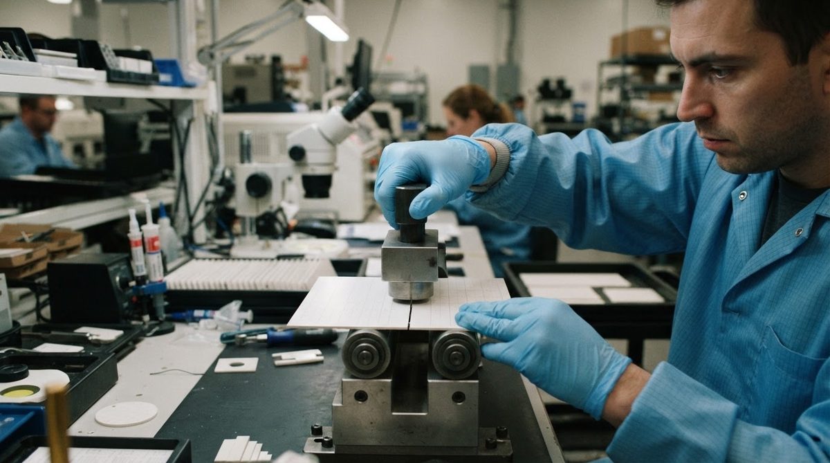
The scribe quality of an aluminum nitride AlN laser scribed panel depends on a handful of tightly coupled parameters. Getting them wrong produces recast debris, excessive HAZ, or incomplete snap separation.
| Parameter | Typical range for AlN | Effect of deviation |
|---|---|---|
| Laser wavelength | 1,064 nm (Nd:YAG) or 355 nm (UV) | UV gives narrower kerf and smaller HAZ but slower throughput |
| Pulse energy | 0.5–5 mJ per pulse | Too high → wide HAZ and recast; too low → incomplete groove |
| Repetition rate | 10–100 kHz | Higher rate increases speed but can cause thermal buildup |
| Scribe depth | 30–70% of substrate thickness | Below 30% → unreliable snap; above 70% → risk of premature fracture |
| Scribe speed | 50–300 mm/s | Slower = deeper groove per pass; faster = more passes needed |
| Number of passes | 1–5 | Multiple passes reduce per-pass thermal load |
Typical values for commercially available equipment. Confirm against your laser vendor’s process sheet for your specific AlN grade and thickness.
UV lasers (355 nm, frequency-tripled Nd:YAG) are increasingly common for aluminum nitride AlN laser scribed work because the shorter wavelength couples more efficiently to the ceramic, producing a kerf width of 20–40 µm versus 50–80 µm for infrared. The trade-off is lower ablation rate, which adds cycle time for thick substrates (≥1.0 mm).
Design Rules for Laser-Scribed AlN Panels
Designing a panel for laser singulation is straightforward, but a few rules prevent yield loss.
- Keep-out from scribe line: Maintain ≥200 µm clearance between any metallization or via and the scribe groove. Recast debris can bridge traces closer than this.
- Minimum part width: Parts narrower than 3 mm after singulation are prone to breakage during snap separation. Below 2 mm, full-cut laser dicing is safer than scribe-and-snap.
- Panel thickness sweet spot: Scribe-and-snap works best on 0.25–1.0 mm AlN. Thicker panels (≥1.5 mm) may need full-depth laser cutting or diamond dicing instead.
- Fiducial placement: Place alignment fiducials at least 1 mm from scribe lines so they survive singulation without chipping.
For thin AlN substrates below 0.25 mm, the scribe depth must be carefully controlled to avoid cutting all the way through during ablation. A single-pass UV scribe at 20–30% depth is typical for 0.15 mm substrates.
Laser Scribing vs. Mechanical Dicing vs. Water-Jet Cutting
| Attribute | Laser scribe + snap | Diamond blade dicing | Water-jet cutting |
|---|---|---|---|
| Dimensional tolerance | ±25–50 µm | ±50–100 µm | ±100–200 µm |
| Edge chipping | Minimal (<20 µm) | Moderate (50–150 µm) | Minimal |
| Subsurface damage | Very low | Moderate | None |
| Kerf width | 20–80 µm | 150–300 µm | 200–500 µm |
| Throughput (parts/hr) | High for thin panels | Moderate | Low |
| Curved cuts possible | Yes | Straight only | Yes |
| Coolant required | No (dry process) | Yes (DI water) | Yes (abrasive slurry) |
Comparative values based on typical production conditions for 0.635 mm AlN substrates.
The dry nature of the aluminum nitride AlN laser scribed process is a significant advantage for substrates that already carry metallization. Diamond dicing requires coolant that can wick under solder mask or contaminate wire-bond pads. Water-jet cutting introduces abrasive garnet particles. Laser scribing sidesteps both issues.
When Laser Scribing Is the Wrong Choice
- Substrate thickness exceeds 1.5 mm. Full-depth laser cutting is slow and generates excessive HAZ. Diamond blade dicing is more practical.
- Complex internal cutouts are needed. Scribe-and-snap only works for straight or gently curved lines. For intricate shapes, full-cut laser or water-jet is required.
- Cost is the primary driver and tolerances are loose. Mechanical dicing is cheaper per cut on thick alumina panels. If you are working with 96% Al₂O₃ rather than AlN, and ±100 µm is acceptable, blade dicing may be the better economic choice. See how to choose the right ceramic substrate for a broader comparison.
- The material is silicon nitride. Si₃N₄ is tougher (fracture toughness ~6–7 MPa·√m vs. ~3 MPa·√m for AlN), which makes the snap step unreliable. Laser-scribed silicon nitride substrates typically require full-depth cutting rather than scribe-and-snap.
Surface Quality After Scribing
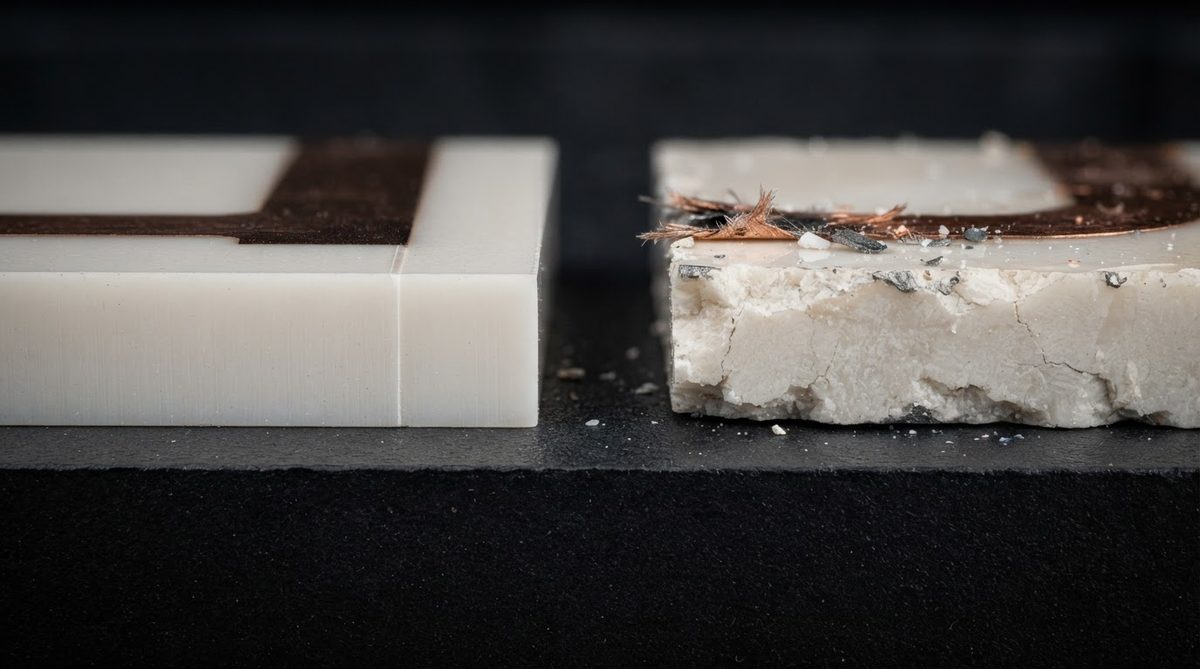
The snapped edge of an aluminum nitride AlN laser scribed substrate shows a characteristic two-zone fracture surface: a smooth laser-ablated groove at the top, and a rougher but clean brittle-fracture face below. Edge roughness (Ra) on the snapped face is typically 1–3 µm, which is adequate for most packaging applications. If a smoother edge is needed—for example, for optical alignment—polished AlN substrates can be post-processed, though this adds cost and cycle time.
Recast (re-deposited ablation debris) along the groove edges is typically <10 µm thick for UV scribing. It can be removed with ultrasonic cleaning in DI water if surface cleanliness is critical for subsequent metallization or die attach.
Material Properties Relevant to Laser Scribing
For full AlN material properties and datasheets, see the dedicated page. The properties most relevant to the aluminum nitride AlN laser scribed process are summarized here.
| Property | Value | Unit | Condition | Source |
|---|---|---|---|---|
| Thermal conductivity | 170–200 | W/mK | 20 °C, >99% dense | Kyocera SH-170 datasheet |
| Flexural strength | 300–350 | MPa | ASTM C1161, 4-pt bend | CoorsTek ADS-995 datasheet |
| Fracture toughness | 2.6–3.5 | MPa·√m | ASTM C1421 | CeramTec Alunit datasheet |
| Optical absorption at 1,064 nm | Moderate | — | Depends on oxygen content | General literature |
| Optical absorption at 355 nm | High | — | Band-gap ~6.2 eV | General literature |
| CTE | 4.5–4.7 | ppm/°C | 20–400 °C | Maruwa HA-200 datasheet |
Typical values for commercially available material, for comparison only. Confirm against the datasheet for your specific grade.
The high UV absorption of AlN (band gap ~6.2 eV) is the reason UV lasers produce cleaner scribes: photon energy at 355 nm (3.5 eV) is absorbed more efficiently at the surface rather than penetrating deep into the bulk, concentrating ablation exactly where it is needed.
FAQ
Does laser scribing affect AlN thermal conductivity?
No. The heat-affected zone is typically under 50 µm wide, confined to the scribe groove that is removed during snap separation. The bulk substrate retains its full 170–200 W/mK conductivity.
Can laser-scribed AlN panels be metallized before singulation?
Yes, and this is the standard workflow. Panels are metallized (DPC, thin film, or thick film), then laser-scribed, then snapped. The dry scribing process avoids coolant contamination of metallized surfaces.
What is the minimum part size achievable with scribe-and-snap on AlN?
Parts as small as 3 × 3 mm are routinely produced at 0.635 mm thickness. Below 3 mm in any dimension, full-depth laser cutting is recommended to avoid fracture during the snap step.
Is laser scribing more expensive than diamond dicing for AlN?
Per-cut cost is similar for thin substrates (≤0.635 mm). Laser scribing becomes more cost-effective at higher volumes because there is no blade wear and no coolant system to maintain. For thick substrates (>1.0 mm), diamond dicing can be cheaper per cut due to faster material removal.
Can I specify curved scribe lines on an AlN panel?
Yes, galvo-scanned laser systems can follow arbitrary 2D paths. However, scribe-and-snap only works reliably along straight lines or very gentle curves (radius >50 mm). For tight curves, full-depth laser cutting is required.