The SiC power module AlN PCB combination has become the standard substrate architecture for high-performance silicon carbide modules. Aluminum nitride delivers 170–200 W/mK thermal conductivity at 20 °C—roughly 6–8× higher than 96% alumina—while its coefficient of thermal expansion (CTE) of 4.4–4.7 ppm/°C closely matches SiC’s 4.0–4.5 ppm/°C. That combination keeps die-attach stress low and thermal resistance minimal at the junction temperatures SiC devices routinely reach: 175 °C and above.
Key Takeaways
- AlN substrates conduct heat at 170–200 W/mK (20 °C), compared to 24–28 W/mK for 96% Al₂O₃, per Kyocera and Maruwa published datasheets.
- The CTE mismatch between AlN (4.4–4.7 ppm/°C) and SiC (4.0–4.5 ppm/°C) is under 0.5 ppm/°C, reducing solder-joint fatigue during thermal cycling.
- SiC MOSFETs from Wolfspeed and Infineon are rated for continuous junction temperatures of 175–200 °C; AlN substrates remain mechanically stable well above 800 °C.
- Direct Bond Copper (DBC) and Active Metal Brazing (AMB) are the two main metallization methods used to bond thick copper to AlN for power module substrates.
- AlN costs 3–5× more per unit area than 96% alumina, so it is justified only when the thermal budget demands it.
Why a SiC Power Module AlN PCB Pairing Works
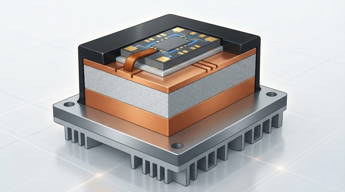
Silicon carbide semiconductors switch faster and tolerate higher temperatures than silicon IGBTs. That advantage is only useful if the substrate underneath can move heat away from the die and survive repeated thermal excursions without cracking the solder joint or delaminating the copper trace.
Two properties make the SiC power module AlN PCB stack the right fit. First, AlN’s thermal conductivity (170–200 W/mK) keeps the substrate’s contribution to total thermal resistance small. Second, its CTE is nearly identical to SiC, so the die-attach interface sees minimal shear stress during the rapid temperature swings that occur every switching cycle. A 96% alumina substrate, by contrast, has a CTE of roughly 7.0–7.4 ppm/°C—almost double that of SiC—which accelerates solder fatigue and limits module lifetime under power cycling.
Thermal Resistance: A Worked Example
Consider a half-bridge SiC MOSFET module dissipating 120 W through a 25 mm × 25 mm substrate footprint. The substrate is 0.635 mm thick AlN with DBC copper on both sides.
Thermal resistance through the substrate alone:
Rth = t / (k × A)
Rth = 0.000635 m / (180 W/mK × 0.000625 m²) = 0.0056 K/W
Temperature rise across the substrate: 120 W × 0.0056 K/W ≈ 0.68 °C.
Now repeat the calculation with 96% alumina (k = 26 W/mK, same geometry):
Rth = 0.000635 / (26 × 0.000625) = 0.039 K/W
Temperature rise: 120 W × 0.039 = 4.7 °C.
The AlN substrate adds less than 1 °C to the thermal stack; the alumina substrate adds nearly 5 °C. In a module already operating at 175 °C junction temperature, that 4 °C difference can be the margin between meeting and missing a reliability target. For details on custom AlN PCB fabrication, including available thicknesses and panel sizes, see our dedicated page.
Enter your own substrate dimensions, material, and dissipated power below to estimate the temperature rise across your SiC power module AlN PCB substrate.
AlN vs. Alumina vs. Si₃N₄ for SiC Power Module PCB Substrates
| Parameter | AlN | 96% Al₂O₃ | Si₃N₄ | Unit | Condition |
|---|---|---|---|---|---|
| Thermal conductivity | 170–200 | 24–28 | 70–90 | W/mK | 20 °C |
| CTE | 4.4–4.7 | 7.0–7.4 | 2.5–3.5 | ppm/°C | 25–400 °C |
| Flexural strength | 300–400 | 300–380 | 600–900 | MPa | ASTM C1161 |
| Dielectric strength | 15–17 | 10–15 | 12–18 | kV/mm | 20 °C |
| Max continuous use temp | ~1 000 | ~1 600 | ~1 000 | °C | In inert/N₂ atmosphere |
| Relative substrate cost | 3–5× | 1× | 4–7× | — | Per cm² at 0.635 mm |
Typical values for commercially available material, for comparison only. Confirm against the datasheet for your specific grade. Sources: Kyocera SN series datasheet, Maruwa AlN-170/AlN-200 datasheet, CoorsTek ADS-996 datasheet.
Si₃N₄ wins on mechanical toughness and is gaining adoption in traction inverters where vibration and thermal shock are extreme. However, its thermal conductivity is roughly half that of AlN, so it demands thinner substrates or larger die pads to hit the same thermal resistance. For most bench-top, industrial, and server-power SiC modules, the SiC power module AlN PCB approach remains the default. To understand how CTE matching in ceramic PCB design affects long-term solder-joint reliability, see our design guide.
DBC vs. AMB Metallization on AlN
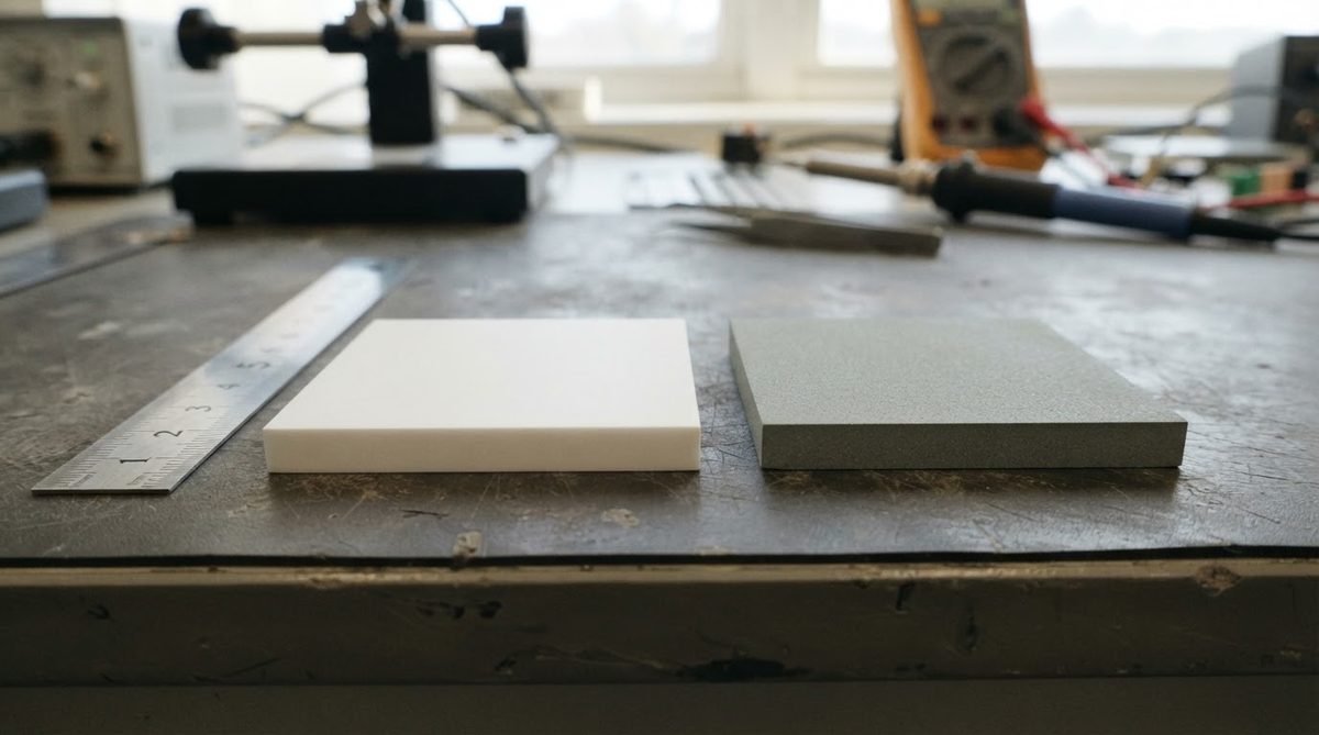
Direct Bond Copper (DBC) bonds copper to AlN through a thin copper-oxide eutectic layer at roughly 1 065 °C. It is the established process for modules rated up to about 150 °C continuous baseplate temperature. Above that, the bond can degrade under aggressive power cycling because the copper-oxide interlayer is relatively thin and brittle.
Active Metal Brazing (AMB) uses a titanium-containing braze alloy (typically AgCuTi) applied between 800–900 °C. The resulting bond is stronger and more fatigue-resistant, which is why AMB-on-AlN is increasingly specified for automotive traction inverters and railway converters where modules see millions of thermal cycles. AMB also allows thicker copper (up to 0.8 mm or more), which reduces trace resistance and improves current handling.
The trade-off is cost: AMB substrates are typically 30–60% more expensive than DBC equivalents at the same copper thickness, driven by the braze material and the vacuum-furnace process. If your module sees fewer than 50 000 power cycles over its life, DBC on AlN is usually sufficient for a reliable SiC power module AlN PCB assembly.
Design Considerations for SiC Power Module AlN PCB Layouts
Solder and die-attach selection
High-lead solders (e.g., Pb93.5Sn5Ag1.5, liquidus ~305 °C) and sintered-silver die attach are the two main options for bonding SiC die to AlN DBC. Sintered silver offers lower thermal resistance (Rth of the bond layer itself drops by roughly 30–50% versus solder) and survives higher junction temperatures, but requires controlled pressure and atmosphere during sintering. For modules operating continuously above 175 °C, sintered silver is the safer choice.
Substrate thickness
Standard AlN DBC substrates come in 0.25 mm, 0.38 mm, and 0.635 mm ceramic thicknesses. Thinner substrates lower thermal resistance but reduce dielectric isolation voltage. At 0.25 mm, an AlN substrate still provides roughly 3.8–4.3 kV of dielectric withstand (based on 15–17 kV/mm dielectric strength), which is adequate for 1200 V SiC modules but leaves little margin for 3.3 kV-class devices. For those, 0.635 mm is typical.
Copper pattern rules
Minimum copper-to-edge clearance on DBC AlN is typically 0.5–1.0 mm to avoid stress concentration at the ceramic edge. Trace spacing for 1200 V isolation should follow IPC-2221B creepage and clearance tables or the module’s target standard (IEC 60664-1). If you need laser-scribed AlN substrates for snap-apart panelization, account for the scribe groove reducing effective edge clearance.
When Not to Use AlN for Your Power Module
AlN is not always the right answer. Consider alternatives in these situations:
- Silicon IGBTs at ≤150 °C junction temperature: 96% alumina DBC is 3–5× cheaper and thermally adequate. See options for 96% alumina substrates.
- Extreme mechanical shock or vibration (automotive traction, rail): Si₃N₄ AMB substrates offer 2–3× the fracture toughness of AlN and are increasingly preferred despite lower thermal conductivity.
- Low-power SiC gate drivers or signal conditioning: Standard alumina or even FR-4 suffices when dissipation is under a few watts.
- Cost-driven consumer products: If the thermal margin is comfortable with an aluminum-core MCPCB, the 10–20× cost difference versus AlN DBC is hard to justify.
Frequently Asked Questions
Does AlN oxidize at high temperatures?
Yes. AlN forms an aluminum oxide layer when exposed to air above roughly 700 °C. In a sealed power module operating at 200 °C baseplate, oxidation is negligible. During metallization processes (DBC, AMB), manufacturers use controlled atmospheres (nitrogen or vacuum) to prevent surface degradation.
Can I use standard SAC305 solder to attach SiC die on AlN DBC?
SAC305 has a liquidus of about 220 °C. If your SiC die runs at 175 °C continuously, the homologous temperature of the solder exceeds 0.9, which causes rapid creep and fatigue. Use high-lead solder (liquidus ~305 °C) or sintered-silver die attach for SiC junctions above 150 °C.
What is the typical lifetime of an AlN DBC substrate under power cycling?
Published data from Infineon and Semikron show AlN DBC substrates surviving 20 000–80 000 power cycles at ΔTj = 100 °C, depending on copper thickness and bond quality. AMB on AlN extends this to 100 000+ cycles under similar conditions. Actual lifetime depends heavily on copper thickness, module geometry, and cooling strategy.
Is Si₃N₄ replacing AlN in SiC modules?
Si₃N₄ is gaining share in automotive traction inverters where mechanical robustness under vibration and extreme thermal cycling is the top priority. For industrial, server-power, and telecom SiC modules, the SiC power module AlN PCB configuration remains dominant because AlN’s thermal conductivity is roughly 2× that of Si₃N₄, and the mechanical demands are less severe.
How does AlN compare to AlSiC baseplates?
AlSiC is a metal-matrix composite used as a baseplate, not a dielectric substrate. A typical SiC power module uses an AlN DBC substrate soldered to an AlSiC baseplate. The AlN provides electrical isolation; the AlSiC provides a CTE-matched heat spreader between the substrate and the heatsink. They are complementary, not competing, layers. For other high-thermal-demand applications of AlN, such as UV LED assemblies, see our page on AlN PCBs for UV LEDs.