An alumina 99.6% Al2O3 HTCC co-fired ceramic substrate is a high-purity ceramic formed by co-firing green tape and refractory metallization (tungsten or moly-manganese) at 1500–1750 °C in a reducing atmosphere. Compared to standard 96% alumina, the higher purity delivers better thermal conductivity (30–35 W/mK vs. 24–28 W/mK at 25 °C), higher volume resistivity, and lower dielectric loss. These advantages matter in RF packaging, high-power modules, and hermetic sensor housings where alumina 99.6% Al2O3 HTCC co-fired ceramic construction provides the reliability that organic boards cannot match.
Key Takeaways
- 99.6% alumina HTCC substrates are sintered at 1500–1750 °C, requiring tungsten or moly-manganese conductors that survive those temperatures.
- Thermal conductivity reaches 30–35 W/mK at 25 °C (per Kyocera A-493 and CoorsTek ADS-996 datasheets), roughly 25–30% higher than 96% alumina.
- Dielectric constant is 9.7–9.9 at 1 MHz, with a loss tangent of 0.0001–0.0003, making the material suitable for low-loss RF signal paths.
- Flexural strength ranges from 350–400 MPa (ASTM C1161, 3-point bend), higher than 96% grades at 300–350 MPa.
- The HTCC process allows buried vias and internal cavities, enabling 3D multilayer packages that are not possible with post-fire metallization methods.
What Is Alumina 99.6% Al2O3 HTCC Co-Fired Ceramic?
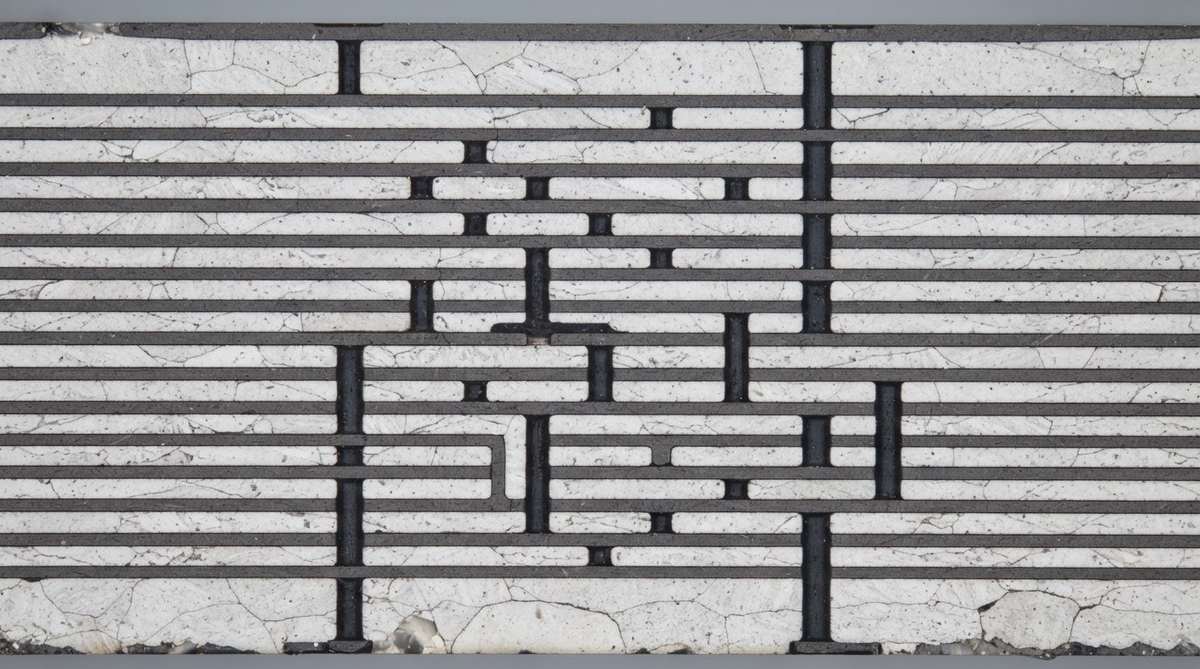
HTCC—high-temperature co-fired ceramic—starts with casting ceramic slurry into thin green tape sheets. Vias are punched, conductor paste (tungsten or moly-manganese) is screen-printed onto each layer, and the stack is laminated under heat and pressure. The entire assembly then sinters together in one firing step at 1500–1750 °C in a hydrogen or forming-gas atmosphere. When the tape is made from 99.6% pure alumina powder, the result is an alumina 99.6% Al2O3 HTCC co-fired ceramic body with minimal glass-phase content and superior electrical and thermal performance.
This contrasts with 99.6% alumina thick film substrates, where a pre-fired blank is metallized afterward at 850–1000 °C. Thick film uses silver, gold, or palladium-silver conductors. Thin film deposits metal by sputtering onto a finished substrate. Each approach has a different conductor set, resolution limit, and cost profile. HTCC’s defining advantage is the ability to embed conductors, vias, and cavities inside the ceramic body itself.
Material Properties of 99.6% Al2O3 HTCC Substrates
| Parameter | Value | Unit | Condition | Source |
|---|---|---|---|---|
| Al2O3 purity | 99.6 | % | — | CoorsTek ADS-996 |
| Density | 3.89–3.92 | g/cm³ | Sintered | Kyocera A-493 |
| Thermal conductivity | 30–35 | W/mK | 25 °C | Kyocera A-493 |
| CTE | 7.1–7.4 | ppm/°C | 25–400 °C | CoorsTek ADS-996 |
| Dielectric constant (εr) | 9.7–9.9 | — | 1 MHz, 25 °C | Kyocera A-493 |
| Loss tangent (tan δ) | 0.0001–0.0003 | — | 1 MHz, 25 °C | CoorsTek ADS-996 |
| Volume resistivity | >1014 | Ω·cm | 25 °C | CoorsTek ADS-996 |
| Flexural strength | 350–400 | MPa | 3-pt bend, ASTM C1161 | Kyocera A-493 |
| Dielectric strength | 25–30 | kV/mm | AC, 25 °C | CoorsTek ADS-996 |
Typical values for commercially available material, for comparison only. Confirm against the datasheet for your specific grade.
99.6% Alumina HTCC vs. 96% Alumina HTCC
The 4-percentage-point difference in purity is mostly about the glass-phase binder. 96% alumina contains more silica and calcia flux to lower sintering temperature and cost. That glass phase sits at grain boundaries and reduces thermal conductivity, increases dielectric loss, and lowers mechanical strength.
For most industrial and automotive applications, 96% alumina HTCC substrates are the cost-effective default. The jump to 99.6% is justified when you need one or more of: lower RF insertion loss above 1 GHz, better hermeticity for long-life implantable or space packages, or tighter dimensional control after sintering (the less glass phase, the more predictable the shrinkage).
| Parameter | 96% Al2O3 | 99.6% Al2O3 | Unit |
|---|---|---|---|
| Thermal conductivity (25 °C) | 24–28 | 30–35 | W/mK |
| Dielectric loss (1 MHz) | 0.0005–0.001 | 0.0001–0.0003 | — |
| Flexural strength | 300–350 | 350–400 | MPa |
| Relative substrate cost | 1× | 1.5–2× | — |
Values from Kyocera and CoorsTek datasheets. Cost multiplier is a rough industry average for equivalent geometry.
Typical Applications for Alumina 99.6% Al2O3 HTCC Co-Fired Ceramic
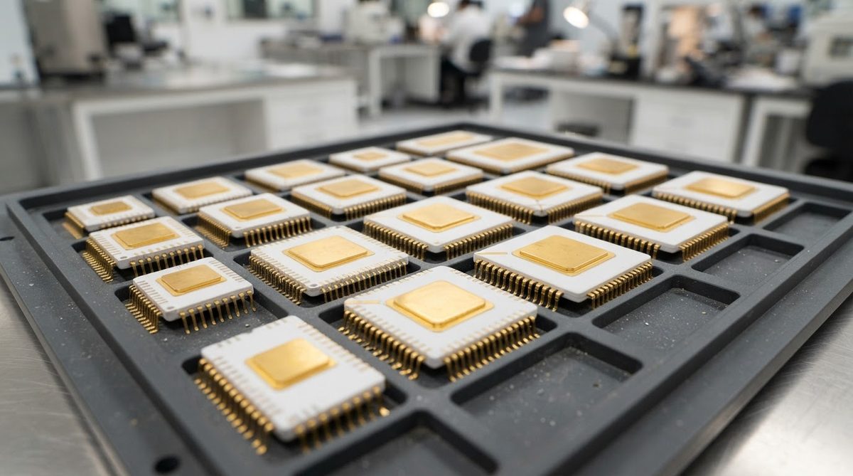
99.6% alumina HTCC substrates appear most often in hermetic microelectronic packages for military, aerospace, and medical devices. The co-fired structure allows a multilayer package with internal routing, seal rings, and brazeable I/O pads—all in a single monolithic body. Common use cases include crystal oscillator housings, MEMS sensor packages, RF power amplifier carriers, and hybrid microcircuit substrates where MIL-PRF-38534 qualification is required.
In RF and microwave work, the low loss tangent keeps signal attenuation in check through Ka-band frequencies. The high dielectric constant does shrink wavelength, which can be an advantage for miniaturization or a constraint for impedance matching—check your line widths early in layout.
Design Considerations for HTCC Co-Fired Ceramic
Conductor Material Limits
Because the substrate sinters above 1500 °C, only refractory metals survive co-firing. Tungsten (W) is the standard HTCC conductor, with a bulk resistivity of about 5.5 µΩ·cm—roughly 3.3× higher than copper. Moly-manganese is used where brazeability matters more than conductivity. Neither matches the performance of gold or silver conductors available in thick film and thin film processes. For high-current paths, this resistivity penalty must be factored into trace sizing.
Shrinkage and Tolerances
HTCC green tape shrinks 15–20% linearly during sintering. Achieving tight feature-to-feature tolerances (below ±0.5% of nominal dimension) requires careful process control and matched-shrinkage tape lots. If your design demands ±25 µm positional accuracy on metallization, consider post-fire laser trimming or switching to a 99.6% alumina thin film substrate where lithographic patterning delivers tighter registration.
Substrate Thickness
HTCC substrates can be built up from multiple green tape layers, so total thickness is flexible. Individual tape layers are typically 100–250 µm green (80–200 µm fired). Check the ceramic substrate thickness chart for standard fired dimensions and tolerances.
When Not to Use 99.6% Al2O3 HTCC
If your application does not require hermeticity, buried vias, or internal cavities, thick film or thin film on a pre-fired 99.6% blank is simpler and cheaper. You skip the tooling for via punching, lamination, and co-fire profile development.
If thermal conductivity above 35 W/mK is essential—power semiconductor modules dissipating more than a few watts per square centimeter—aluminum nitride (170–200 W/mK) is the right material. An AlN thick film substrate or AMB assembly will outperform any alumina grade thermally.
If cost is the primary driver and the operating environment is benign (below 150 °C, no hermeticity needed), FR-4 or metal-core PCBs will do the job at a fraction of the price. Ceramic substrates earn their premium in harsh environments—high temperature, corrosive atmosphere, high voltage, or long service life—where organic boards cannot survive.
Frequently Asked Questions
What conductor metals work with alumina 99.6% Al2O3 HTCC co-fired ceramic?
Tungsten and moly-manganese are the standard choices because they withstand sintering temperatures above 1500 °C. Gold, silver, and copper cannot survive the co-firing step. Post-fire plating (nickel/gold) is added afterward for solderability and wire bonding.
Can I get 99.6% alumina in LTCC instead of HTCC?
No. LTCC (low-temperature co-fired ceramic) uses glass-ceramic tape systems that sinter at 850–900 °C. These materials are not high-purity alumina; they are proprietary glass-alumina or glass-cordierite blends with very different properties. If you need 99.6% alumina, HTCC is the co-fired route.
How does the CTE of 99.6% alumina compare to silicon?
99.6% alumina has a CTE of 7.1–7.4 ppm/°C (25–400 °C), while silicon is about 2.6 ppm/°C over the same range. The mismatch is manageable for small die (under ~8 mm) with compliant solder or epoxy attach, but large die may need AlN (CTE 4.5 ppm/°C) for a closer match.
Is 99.6% alumina HTCC suitable for vacuum or hermetic packages?
Yes. Dense 99.6% alumina is inherently hermetic after full sintering, with helium leak rates below 1 × 10⁻⁹ atm·cc/sec achievable per MIL-STD-883 Method 1014. The co-fired structure eliminates joints between substrate and metallization, which improves long-term seal integrity compared to post-fire brazing.
What is the maximum operating temperature?
The ceramic body itself is stable well above 1000 °C. The practical limit is set by the metallization and any attached solder or braze joints. Tungsten metallization remains functional to roughly 800–1000 °C in inert or reducing atmospheres. In oxidizing air, tungsten oxidizes above about 400 °C, so protective overcoats or hermetic sealing are required for high-temperature air exposure.