An alumina 96% Al2O3 thin film ceramic substrate is a polycrystalline ceramic base with vacuum-deposited metal layers—typically sputtered Ti/Pt/Au or TaN/NiCr resistor films—patterned by photolithography to achieve line and space widths down to 10/10 µm. It is the workhorse substrate for hybrid microelectronics, sensor circuits, and RF thin film networks where cost matters more than ultimate thermal conductivity. If you are evaluating alumina 96% Al2O3 thin film ceramic for a new design, the sections below cover properties, trade-offs, and practical design guidance.
Key Takeaways
- 96% Al2O3 thin film substrates provide thermal conductivity of 24–28 W/mK at 20 °C, adequate for most low-to-moderate power density circuits.
- Thin film metallization enables feature sizes of 10/10 µm line/space, far finer than thick film’s typical 100/100 µm minimum.
- Surface finish (Ra) of the bare substrate must be ≤ 0.05 µm (50 nm) for reliable thin film adhesion; lapped and polished 96% alumina meets this.
- 96% alumina costs roughly 30–50% less per unit area than 99.6% alumina, making it the default choice unless tighter dielectric or thermal specs demand higher purity.
- Dielectric strength is typically 10–15 kV/mm per ASTM D149, sufficient for most sub-1 kV isolation requirements.
Material Properties of Alumina 96% Al2O3 Thin Film Ceramic
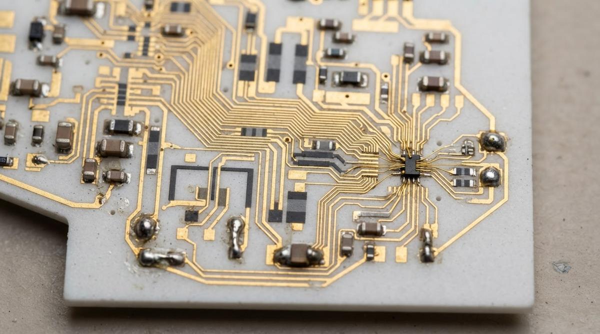
The “96%” designation means the substrate is approximately 96% Al2O3 by weight, with the balance being sintering aids—primarily silica, calcia, and magnesia. These additives lower the firing temperature but also reduce thermal conductivity and introduce a glassy grain-boundary phase that slightly increases dielectric loss at microwave frequencies.
| Parameter | Value | Unit | Condition | Source |
|---|---|---|---|---|
| Thermal conductivity | 24–28 | W/mK | 20 °C, ASTM E1461 | CoorsTek ADS-96R datasheet |
| Dielectric constant (εr) | 9.0–9.5 | — | 1 MHz, 25 °C | Kyocera A-493 datasheet |
| Loss tangent (tan δ) | 0.0002–0.0004 | — | 1 MHz, 25 °C | Kyocera A-493 datasheet |
| Flexural strength | 350–380 | MPa | ASTM C1161, 4-pt bend | CoorsTek ADS-96R datasheet |
| CTE | 7.1–7.4 | ppm/°C | 25–300 °C | CoorsTek ADS-96R datasheet |
| Volume resistivity | >1014 | Ω·cm | 25 °C | CoorsTek ADS-96R datasheet |
| Surface roughness (polished) | 0.02–0.05 | µm Ra | After lapping/polishing | Maruwa HA-96 datasheet |
Typical values for commercially available material, for comparison only. Confirm against the datasheet for your specific grade.
Why Choose Alumina 96% Al2O3 Thin Film Ceramic Over Other Grades?
Thin film processing—sputtering or evaporation followed by photolithographic patterning and wet/dry etching—demands a substrate with low surface roughness, chemical inertness, and dimensional stability through repeated vacuum and thermal cycles. Polished 96% alumina meets all three requirements at a lower price point than 99.6% alumina or aluminum nitride.
Common thin film metal stacks on alumina 96% Al2O3 thin film ceramic substrates include Ti/Pt/Au for wire-bondable conductors, TaN for precision resistors (25–200 Ω/sq sheet resistance, ±0.5% tolerance after laser trimming), and NiCr for lower TCR resistor applications. The glassy grain-boundary phase in 96% alumina can occasionally cause micro-pitting after aggressive cleaning, so incoming substrate inspection is important. Specify a maximum defect density per IPC-6012 or your own workmanship standard.
96% vs. 99.6% Alumina for Thin Film Applications
The decision between 96% and 99.6% alumina comes down to three factors: thermal conductivity, dielectric loss at high frequency, and surface quality.
| Parameter | 96% Al2O3 | 99.6% Al2O3 | Unit |
|---|---|---|---|
| Thermal conductivity (20 °C) | 24–28 | 28–35 | W/mK |
| εr (1 MHz) | 9.0–9.5 | 9.7–9.9 | — |
| tan δ (1 MHz) | 0.0002–0.0004 | 0.0001–0.0002 | — |
| Surface roughness (polished) | 0.02–0.05 | 0.01–0.025 | µm Ra |
| Relative substrate cost | 1× | 1.5–2× | — |
Typical values for commercially available material, for comparison only. Confirm against the datasheet for your specific grade.
For circuits operating below 3 GHz with power densities under roughly 5 W/cm², 96% alumina is usually the right pick. The cost savings compound quickly across production volumes. Above 10 GHz, or where you need tighter resistor tolerance or lower insertion loss, step up to a 99.6% Al2O3 thin film ceramic substrate.
Design Considerations for Thin Film on 96% Alumina
Substrate Thickness Selection
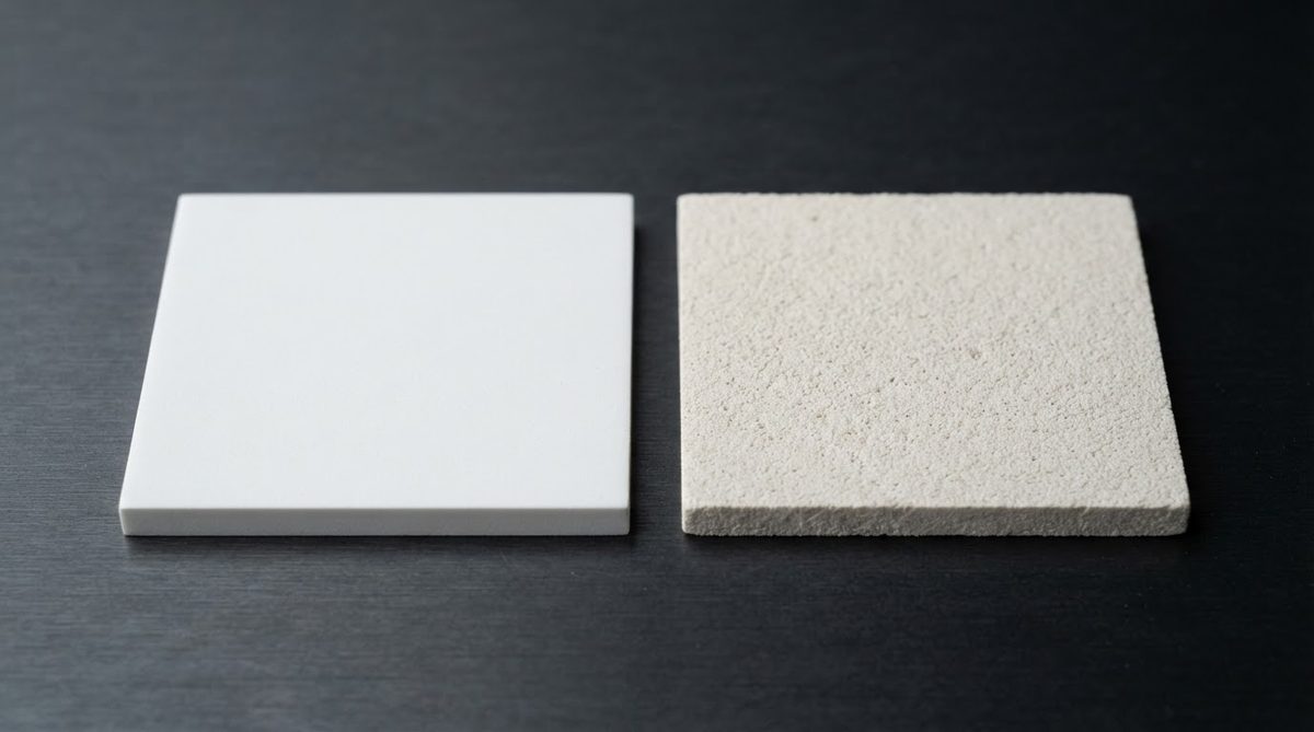
Standard thicknesses range from 0.25 mm to 1.0 mm. Thinner substrates (0.25–0.38 mm) improve thermal resistance through the ceramic but are more fragile during handling and die attach. A ceramic substrate thickness chart helps match your mechanical and thermal requirements to available stock sizes.
Metallization Adhesion
Thin film adhesion on 96% alumina depends heavily on surface preparation. A typical process flow is ultrasonic clean → O2 plasma ash → sputter Ti adhesion layer (20–50 nm) → sputter conductor (Au, Cu, or Pt). Pull-test adhesion should exceed 20 MPa per MIL-STD-883 Method 2011. The glassy phase in 96% alumina can actually help adhesion compared to very pure alumina, because the amorphous surface layer provides more bonding sites for the Ti adhesion layer.
Thermal Resistance Worked Example
Consider a 10 mm × 10 mm die on a 0.635 mm thick alumina 96% Al2O3 thin film ceramic substrate. Thermal resistance through the ceramic alone:
Rth = t / (k × A) = 0.000635 / (26 × 0.0001) = 0.244 °C/W
At 5 W dissipation, the temperature drop across the substrate is about 1.2 °C. For most thin film hybrid circuits, the substrate’s thermal resistance is a small fraction of the total junction-to-ambient path. This is why 96% alumina’s slightly lower conductivity compared to 99.6% rarely matters in practice.
Enter your own substrate dimensions, thickness, and dissipated power below to estimate the temperature rise across your specific alumina 96% Al2O3 thin film ceramic layout.
When Not to Use 96% Alumina Thin Film Substrates
High power density (>15 W/cm²): If you need to spread heat aggressively under power devices, aluminum nitride thin film substrates at 170–200 W/mK are a better match, despite the 5–8× cost premium.
Millimeter-wave RF (>30 GHz): The higher loss tangent and surface roughness of 96% alumina increase insertion loss at mmWave. Consider 99.6% alumina or quartz substrates.
High mechanical shock or thermal cycling: Alumina is brittle. For automotive power modules subjected to –40 °C to +150 °C cycling, silicon nitride AMB substrates offer far higher fracture toughness (6–7 MPa·√m vs. alumina’s 3.5–4 MPa·√m).
Cost-driven consumer electronics: If your circuit has no thermal, frequency, or hermeticity requirement that demands ceramic, FR-4 or metal-core PCB will cost a fraction of the price.
Frequently Asked Questions
What is the maximum operating temperature of a 96% alumina thin film substrate?
The ceramic itself is stable well above 1 000 °C. The practical limit is set by the metallization: Ti/Pt/Au thin films are typically rated to 300–350 °C continuous, while TaN resistor films may drift above 250 °C. Design your thermal budget around the metal stack, not the ceramic.
Can I get 96% alumina substrates with through-holes or vias?
Yes. Laser drilling or mechanical punching before sintering can produce vias down to 0.1–0.15 mm diameter. However, via metallization on thin film substrates adds process steps and cost. For multilayer via-intensive designs, an HTCC co-fired ceramic approach is often more practical.
How does thin film differ from thick film on the same 96% alumina?
Thick film uses screen-printed pastes fired at 850 °C, achieving roughly 100/100 µm line/space. Thin film uses vacuum deposition and photolithography, reaching 10/10 µm. Thin film resistors hold ±0.1–0.5% tolerance after trimming; thick film typically holds ±1–5%. For a comparison of thick film processing on higher-purity alumina, see 99.6% Al2O3 thick film ceramic substrates.
Is 96% alumina suitable for hermetic packaging?
Yes. 96% alumina is widely used in hermetic hybrid packages per MIL-PRF-38534. The substrate’s helium leak rate can meet 1 × 10⁻⁸ atm·cc/sec when properly brazed to a metal seal ring. The glassy grain-boundary phase does not compromise hermeticity at standard package sizes.
What surface finish should I specify for thin film deposition?
Specify Ra ≤ 0.05 µm (50 nm) on the deposition side. Rougher surfaces cause thin film discontinuities and resistor value scatter. Most suppliers offer “as-fired” (Ra 0.3–0.8 µm), “lapped” (Ra 0.1–0.2 µm), and “polished” (Ra 0.02–0.05 µm). Only polished grade is suitable for thin film.
Next Step
If alumina 96% Al2O3 thin film ceramic fits your thermal and electrical requirements, request a ceramic substrate sample kit to validate your thin film process on actual material before committing to production quantities. Include your target thickness, surface finish, and metallization stack in the request for the fastest turnaround.