The loss tangent ceramic substrate range spans roughly two orders of magnitude — from 0.0001 for fused quartz to 0.006 for standard 96% alumina, measured at 1–10 GHz and 25 °C. That spread means material selection directly sets your insertion loss budget, and picking the wrong ceramic can cost you more dB per centimeter than a marginal amplifier stage can recover.
Key Takeaways
- Fused quartz (SiO₂) offers the lowest loss tangent among common ceramic substrates: 0.0001–0.0002 at 10 GHz (per CoorsTek and Kyocera datasheets).
- 99.6% alumina (Al₂O₃) achieves tan δ of 0.0002–0.001 at 10 GHz depending on grain size and purity — a strong mid-range option.
- 96% alumina, the workhorse grade, sits at 0.001–0.006 at 10 GHz — adequate for many RF circuits but not for low-loss mmWave lines.
- Aluminum nitride (AlN) has a tan δ of 0.001–0.003 at 10 GHz; its thermal conductivity (170–200 W/mK) makes it useful for high-power RF, but it is not the lowest-loss option.
- Loss tangent rises with frequency, temperature, and impurity content. Always confirm values at your actual operating frequency, not the 1 MHz figure on a generic datasheet.
What Is Loss Tangent and Why It Matters for Ceramic Substrates
Loss tangent, also called dissipation factor (Df), is the ratio of the imaginary to the real part of a material’s complex permittivity: tan δ = ε″/ε′. It quantifies how much electromagnetic energy the dielectric absorbs and converts to heat per cycle. A lower tan δ means less signal attenuation per unit length of transmission line.
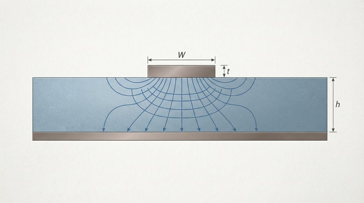
For a microstrip line on a ceramic substrate, the dielectric loss component of total attenuation (α_d) in dB/cm is approximated by:
α_d ≈ 27.3 × (ε_eff / ε_r) × (tan δ / λ₀) × √ε_eff
where ε_r is the substrate’s relative permittivity, ε_eff is the effective permittivity of the microstrip mode, and λ₀ is the free-space wavelength. At 28 GHz (λ₀ ≈ 10.7 mm), even a modest increase in tan δ from 0.0002 to 0.002 multiplies dielectric loss by roughly 10×. That difference can push a filter or feed network out of spec.
Loss Tangent Ceramic Substrate Comparison Table
| Material | tan δ | Frequency | Dk (ε_r) | Temp | Source |
|---|---|---|---|---|---|
| Fused quartz (SiO₂) | 0.0001–0.0002 | 10 GHz | 3.78 | 25 °C | CoorsTek / Kyocera datasheets |
| Sapphire (single-crystal Al₂O₃) | 0.0001–0.0003 | 10 GHz | 9.4–11.6 (anisotropic) | 25 °C | Kyocera sapphire datasheet |
| Al₂O₃ 99.6% | 0.0002–0.001 | 10 GHz | 9.8–9.9 | 25 °C | CoorsTek ADS-996, Kyocera A-493 |
| Al₂O₃ 96% | 0.001–0.006 | 10 GHz | 9.4–9.6 | 25 °C | CoorsTek ADS-96R, Maruwa HA-96 |
| AlN | 0.001–0.003 | 10 GHz | 8.5–8.9 | 25 °C | Maruwa SH-AlN, Kyocera AN-230 |
| Borosilicate glass | 0.001–0.004 | 1–10 GHz | 4.0–5.1 | 25 °C | Schott Borofloat 33 datasheet |
| LTCC (typical) | 0.001–0.005 | 10 GHz | 5.0–9.0 | 25 °C | Ferro A6M / DuPont 951 datasheets |
| Rogers RO4003C (organic, for reference) | 0.0027 | 10 GHz | 3.38 | 25 °C | Rogers Corp. datasheet |
Typical values for commercially available material, for comparison only. Confirm against the datasheet for your specific grade.
How Loss Tangent Changes with Frequency and Temperature
Loss tangent is not a fixed number. For polycrystalline alumina, tan δ at 77 GHz can be 2–5× the value measured at 1 GHz, depending on grain boundary phases and residual glassy content. This frequency dependence is driven by ionic and dipolar relaxation mechanisms in the ceramic matrix. Single-crystal substrates like sapphire show far less frequency dispersion because they lack grain boundaries.
Temperature also matters. Alumina’s tan δ roughly doubles between 25 °C and 200 °C. If your module dissipates significant power — common in GaN PA stages — the substrate heats up, loss rises, more heat is generated, and you enter a mild positive-feedback loop. This is one reason AlN gets chosen for power amplifier pallets despite its higher tan δ at room temperature: its 170–200 W/mK thermal conductivity keeps the substrate cooler, so the effective loss tangent of the ceramic substrate under load stays lower than a hotter alumina substrate would exhibit.
Worked Example: Dielectric Loss at 28 GHz on 96% vs. 99.6% Alumina
Assume a 50 Ω microstrip on a 0.254 mm (10 mil) thick substrate, operating at 28 GHz. Comparing the loss tangent of each ceramic substrate grade illustrates the real-world impact.
- 96% Al₂O₃: ε_r = 9.5, tan δ = 0.004 at 28 GHz (interpolated from manufacturer data). ε_eff ≈ 6.5 (calculated). α_d ≈ 0.18 dB/cm.
- 99.6% Al₂O₃: ε_r = 9.9, tan δ = 0.0006 at 28 GHz. ε_eff ≈ 6.8. α_d ≈ 0.03 dB/cm.
Over a 3 cm feed network, that is 0.54 dB vs. 0.09 dB of dielectric loss alone. For a phased-array element where every 0.1 dB of loss degrades EIRP, the 99.6% grade pays for itself. The substrate cost difference is roughly 2–3× per piece, but the system-level performance gain is decisive at 28 GHz and above.
Use the calculator below to check how substrate permittivity and thickness affect your microstrip impedance and effective permittivity for a given trace width.
[pcb_calc type=”microstrip-impedance”]
How Metallization Affects Total Line Loss
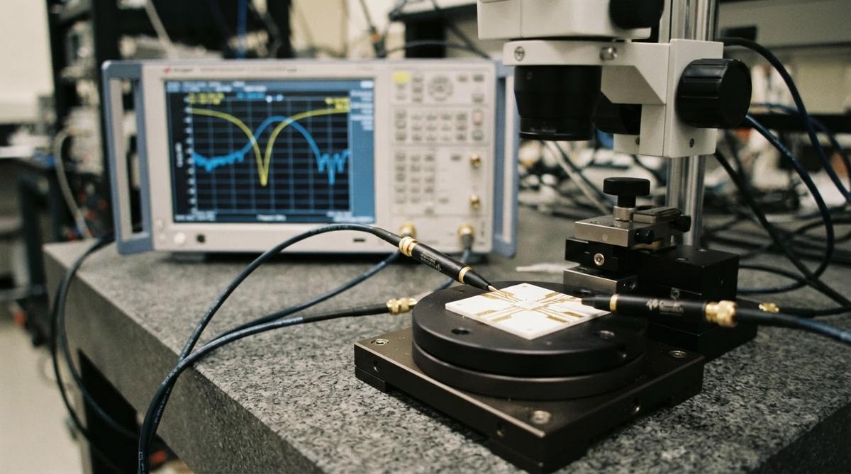
Dielectric loss is only one component. Conductor loss (α_c) from the metallization layer often dominates below 10 GHz and remains significant through mmWave. Thin-film gold or copper on polished ceramic gives the lowest conductor loss because surface roughness is minimized. Thick-film metallization (screen-printed silver or gold) has higher surface roughness (Ra > 1 µm typical), which increases conductor loss at frequencies above a few GHz due to the skin-effect interaction with surface features.
For mmWave circuits, pairing a low-loss-tangent ceramic substrate with thin-film gold metallization on polished 99.6% alumina or quartz is the standard approach. Thick-film processes are adequate for circuits operating below roughly 6 GHz where conductor roughness is less critical.
Choosing the Right Loss Tangent Ceramic Substrate for Your Frequency Band
Below 6 GHz
96% alumina with thick-film metallization handles most applications. Its tan δ of 0.001–0.003 at these frequencies contributes modest dielectric loss, and the substrate cost is the lowest of the ceramic options.
6–30 GHz
Move to 99.6% alumina or AlN. Thin-film metallization becomes important. If thermal management is a priority (power amplifiers, GaN devices), AlN’s thermal conductivity justifies its higher tan δ relative to 99.6% alumina.
Above 30 GHz (mmWave and beyond)
Quartz substrates or sapphire are preferred for passive circuits, filters, and feed networks where loss must be minimized. Their low Dk (3.78 for quartz) also eases impedance matching and widens trace geometries, which improves manufacturing yield.
When Not to Use a Ceramic Substrate for RF
Ceramic is not always the right answer. Standard FR-4 works fine for digital and low-frequency analog below 1 GHz where dielectric loss is negligible. High-frequency laminates like Rogers RO4003C or RO3003 offer tan δ of 0.001–0.003 at 10 GHz with far easier mechanical processing — drilling, routing, and panelization are straightforward. If your circuit does not need the thermal conductivity, hermeticity, or dimensional stability of ceramic, a PTFE or hydrocarbon laminate will cost less and ship faster. Ceramic substrates also cannot be easily routed into complex outlines without laser cutting, which adds cost and lead time.
For multilayer builds with embedded passives, LTCC is the ceramic option — but its tan δ (0.001–0.005 at 10 GHz) is higher than monolithic quartz or 99.6% alumina, so it suits integration-driven designs more than ultra-low-loss ones.
Frequently Asked Questions
Does alumina purity directly correlate with loss tangent?
Yes. Higher purity means fewer glassy-phase grain boundary impurities, which are the primary source of dielectric loss in polycrystalline alumina. 99.6% alumina typically has 5–20× lower tan δ than 96% alumina at 10 GHz. The cost premium is roughly 2–3× per substrate.
Can I use AlN for a low-loss mmWave filter?
AlN’s tan δ of 0.001–0.003 at 10 GHz is higher than 99.6% alumina or quartz, so it is not the best choice for a passive filter where insertion loss is the primary figure of merit. AlN excels where you need both moderate RF performance and high thermal conductivity for active devices.
Is the 1 MHz loss tangent on a datasheet useful for RF design?
No. The 1 MHz value can be 5–10× lower than the value at your actual operating frequency. Always request or look up tan δ at the frequency closest to your operating band. Reputable substrate suppliers like Kyocera and CoorsTek publish data at 1 GHz and 10 GHz.
How does surface roughness interact with loss tangent on a ceramic substrate?
Surface roughness primarily affects conductor loss, not dielectric loss. However, the two losses add together to give total line attenuation. A loss tangent ceramic substrate with excellent tan δ paired with rough thick-film metallization can still produce high total loss at mmWave frequencies. Specify both substrate grade and metallization process together.
What test method measures loss tangent for ceramics?
The split-post dielectric resonator (SPDR) method per IEC 61189-2-721 is widely used for flat substrates at specific GHz frequencies. Cavity perturbation methods (ASTM D2520) and Hakki-Coleman resonators are also common. Each method has different accuracy and frequency range — specify which was used when comparing vendor data.
Next Step
Check the ceramic substrate datasheet library for tan δ values at your target frequency, then request a quote with your Gerber files and frequency requirements so we can recommend the right grade and metallization for your loss budget.