Thick film ceramic design rules center on the screen-printing process: minimum trace width and spacing of 100–125 µm (4–5 mil), conductor thickness of 8–15 µm per print pass, and via diameters starting at 150–200 µm depending on substrate thickness. These numbers are tighter than standard FR-4 but looser than thin film ceramic design rules, which reach below 25 µm trace/space. Understanding where thick film excels—and where it doesn’t—prevents costly redesigns.
Key Takeaways
- Minimum trace width and spacing for thick film is typically 100–125 µm (4–5 mil); tighter features require thin film processes.
- Each screen-print pass deposits 8–15 µm of conductor; multiple passes can build up to 30–40 µm total.
- Thick film resistors can be laser-trimmed to ±1% tolerance, compared with ±10–20% as-printed.
- Via diameters start at 150–200 µm and must be filled with compatible paste for reliable multilayer interconnects.
- 96% alumina (Al₂O₃) is the most common substrate; 99.6% alumina is used when surface finish or hermeticity demands are higher.
What Is Thick Film on Ceramic?
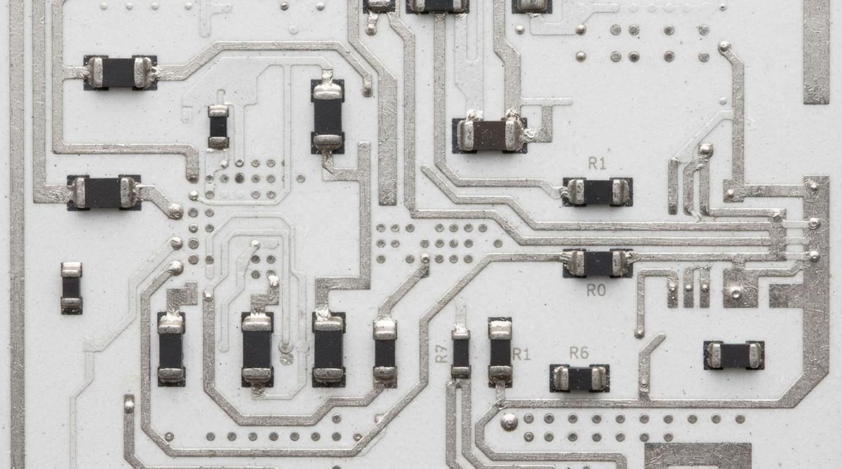
Thick film is an additive process. Conductive, resistive, or dielectric pastes are screen-printed through a patterned stainless-steel mesh onto a fired ceramic substrate, then dried and sintered at 850–1000 °C in a belt furnace. The resulting conductors are dense metallic films—typically silver, gold, palladium-silver, or platinum-gold—bonded directly to the alumina surface.
Because thick film is additive rather than subtractive, there is no etching step. Line definition is governed by screen mesh count, emulsion thickness, and paste rheology. This makes thick film well suited for hybrid circuits, power modules, heater elements, and sensor substrates where embedded resistors or moderate conductor density is needed.
Conductor Design Rules
| Parameter | Typical Rule | Unit | Notes |
|---|---|---|---|
| Min trace width | 100–125 | µm | Finer with high-mesh screens (400 mesh) |
| Min trace spacing | 100–125 | µm | Paste bleed sets the practical floor |
| Conductor thickness (per pass) | 8–15 | µm | After firing; wet print is ~25 µm |
| Max conductor thickness | 30–40 | µm | 2–3 print passes with intermediate drying |
| Sheet resistance (Ag conductor) | 2–5 | mΩ/□ | Per DuPont 6160 / Heraeus C8729 datasheets |
| Line width tolerance | ±15–25 | µm | Depends on screen tension and snap-off |
| Positional accuracy | ±25–50 | µm | Fiducial-aligned printers achieve ±25 µm |
Typical values for commercially available materials and equipment, for comparison only. Confirm against the datasheet for your specific paste and screen supplier.
Conductor width below 100 µm is possible with specialized fine-line screens (400+ mesh, thin emulsion), but yield drops and cost rises. If your design needs traces below 75 µm, switch to thin film or DPC.
Paste Selection Affects Geometry
Silver-based pastes print the finest lines because of their rheology and particle size distribution. Gold and platinum-gold pastes tend to spread slightly more, so add 10–15 µm to your minimum trace width when using these materials. Palladium-silver is a cost compromise but has higher sheet resistance (8–15 mΩ/□), which matters for high-current paths.
Via and Interconnect Rules
Thick film vias are punched or laser-drilled in the green (unfired) ceramic tape for LTCC builds, or drilled in the fired substrate and then filled with conductive paste. For fired-substrate thick film, via diameter starts at 150–200 µm with a minimum land diameter of 300–400 µm. Aspect ratios above 1:1 (depth to diameter) are difficult to fill reliably.
Paste fill must be compatible with the conductor paste to avoid delamination or cracking during firing. For designs requiring high via density or blind/buried vias, consult the guidance on ceramic via filling techniques before committing to a stackup.
Thick Film Resistor Design Rules
Embedded resistors are one of thick film’s strongest advantages over competing processes. Resistive pastes are available in decade values from 1 Ω/□ to 10 MΩ/□. The resistor value is set by the aspect ratio (length ÷ width) of the printed rectangle multiplied by the paste’s sheet resistance.
Worked Example: Sizing a 10 kΩ Resistor
Using a 10 kΩ/□ paste, a 1:1 square (equal length and width) gives exactly 10 kΩ. To hit 47 kΩ, you need an aspect ratio of 4.7:1. If the minimum printable width is 200 µm, the resistor body would be 200 µm wide × 940 µm long. Add 150 µm overlap pads on each end for conductor contact, giving a total footprint of roughly 200 µm × 1240 µm.
| Parameter | Rule | Unit | Notes |
|---|---|---|---|
| Min resistor width | 200 | µm | Narrower prints have poor tolerance |
| Min resistor length | 200 | µm | 1:1 aspect ratio minimum |
| Max aspect ratio | 10:1 | — | Beyond this, use serpentine or higher Ω/□ paste |
| As-printed tolerance | ±10–20 | % | Varies with paste lot and print quality |
| Laser-trimmed tolerance | ±0.5–1 | % | Functional trim under power preferred |
| TCR (typical RuO₂ paste) | ±100–200 | ppm/°C | Per DuPont 2000 series datasheet |
| Conductor overlap | ≥150 | µm | Resistor must overlap onto conductor pad |
Typical values for commercially available material, for comparison only. Confirm against the datasheet for your specific grade.
Place resistors away from substrate edges (≥500 µm) and away from vias. Thermal gradients near edges and via barrels shift resistance values unpredictably. For detailed placement guidance, refer to the thick film layout and placement guide.
Substrate Selection
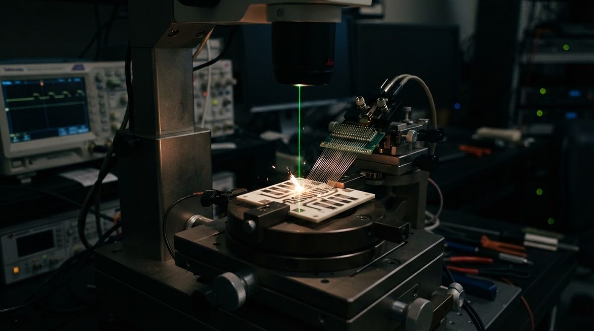
96% alumina is the default substrate for thick film. It costs roughly one-third of 99.6% alumina, fires at compatible temperatures, and offers 24–28 W/m·K thermal conductivity (per CoorsTek ADS-96R datasheet, measured at 25 °C per ASTM E1461). Surface roughness of 96% alumina (Ra 0.3–0.6 µm, as-fired) is adequate for 100 µm trace widths.
99.6% alumina is chosen when you need a smoother surface (Ra < 0.1 µm after lapping), better hermeticity, or higher dielectric strength. For 99.6% alumina thick film substrates, the finer grain structure allows marginally tighter print resolution, but the cost premium rarely justifies it unless the application demands it.
Multilayer Thick Film Stackups
Thick film can be built up in multiple print-and-fire cycles on a single substrate: print conductor layer 1, fire, print dielectric, fire, print conductor layer 2, fire. Each dielectric layer adds roughly 30–50 µm and must be pinhole-free to prevent shorts. Practical layer counts max out at 3–4 conductor layers before cumulative registration error and dielectric defects become yield-limiting.
For designs needing five or more conductor layers, LTCC co-fired tape technology or a multilayer ceramic PCB stackup is a better path. LTCC fires all layers simultaneously, eliminating cumulative alignment drift.
When Not to Use Thick Film
Thick film is the wrong process in several common scenarios:
- Trace/space below 75 µm. Thin film (sputter + photolithography) or DPC achieves 20–25 µm features routinely.
- High-frequency RF above 10 GHz. Thick film conductor edges are rough (±15–25 µm), increasing insertion loss. Thin film or DPC gives the edge definition RF circuits need.
- High current (>5 A per trace). Thick film conductors max out at 30–40 µm. If you need 50–300 µm copper, look at DBC, AMB, or plated copper on ceramic.
- No embedded passives needed and tight geometry required. If you don’t need printed resistors and your design is fine-pitch, thin film is faster and more precise.
- Cost-sensitive, low-temperature applications. FR-4 or metal-core PCBs cost a fraction of ceramic thick film. If the operating environment stays below 130 °C and thermal conductivity above 1–2 W/m·K is enough, ceramic is overkill.
Frequently Asked Questions
What is the finest line a thick film screen can print?
Production-grade thick film screens reliably resolve 100–125 µm (4–5 mil) traces and spaces. Specialty fine-line screens with 400+ mesh can push to 75 µm, but yield is lower and cost per panel increases. Below 75 µm, thin film is the standard approach.
Can thick film resistors replace discrete SMD resistors?
Yes, and this is one of thick film’s primary advantages. Laser-trimmed thick film resistors reach ±0.5–1% tolerance with TCR of ±100 ppm/°C, which is adequate for most analog signal conditioning, voltage dividers, and sensor bridges. They also eliminate solder joints, improving long-term reliability in high-vibration environments.
How many conductor layers can I stack in thick film?
Three to four conductor layers is the practical limit for sequential print-and-fire thick film. Each additional layer adds registration error (±25–50 µm per layer) and requires a defect-free dielectric print. Beyond four layers, LTCC co-fired multilayer technology is more reliable and often more cost-effective at volume.
Does thick film work on aluminum nitride (AlN)?
It can, but paste chemistry must be specifically formulated for AlN. Standard alumina thick film pastes contain glass frits that do not bond well to AlN surfaces. Specialized AlN-compatible pastes (e.g., from Heraeus or Tanaka) are available but cost more and have a narrower process window. Most thick film production uses alumina substrates.
What firing temperature does thick film require?
Standard thick film pastes fire at 850–1000 °C in air, with a peak hold time of 8–12 minutes in a belt furnace. This is well below the sintering temperature of alumina (~1600 °C), so the substrate is unaffected. Low-temperature pastes (firing at 600–700 °C) exist for polymer thick film, but these have lower conductivity and durability.
Next Step
If your design fits within 100 µm trace/space and benefits from embedded resistors, thick film on alumina is likely the right process. Prepare your Gerber files with the rules above, then request a design review and quote to confirm manufacturability for your specific layout.