Thick copper ceramic PCBs carry copper layers from roughly 100 µm to 300 µm (and sometimes beyond) bonded directly to a ceramic substrate. They handle high current densities, spread heat efficiently from power devices, and survive thermal cycling that would delaminate organic laminates. The trade-off is cost, minimum feature size, and the engineering required to manage CTE mismatch between copper (17 ppm/K) and ceramic (6–8 ppm/K for Al₂O₃, 4.5 ppm/K for AlN).
Key Takeaways
- Direct Bond Copper (DBC) delivers 200–300 µm copper on Al₂O₃ or AlN in a single firing step, with peel strength above 4 N/mm per CeramTec datasheet.
- Active Metal Brazing (AMB) bonds copper up to 800 µm to Si₃N₄ or AlN, surviving >3 000 thermal cycles (–40 °C to +150 °C) per Kyocera reliability data.
- Electroplated copper on ceramic can build up from a seed layer to 50–200 µm, offering finer trace resolution than DBC but lower throughput.
- Thick-film printed copper tops out around 20–50 µm per print-fire pass; multiple passes can reach ~100 µm but with diminishing adhesion and resolution.
- Minimum trace/space widens as copper gets thicker: expect ≥300 µm trace/space at 300 µm copper versus ≤50 µm at 10 µm copper.
Methods for Putting Thick Copper on Ceramic
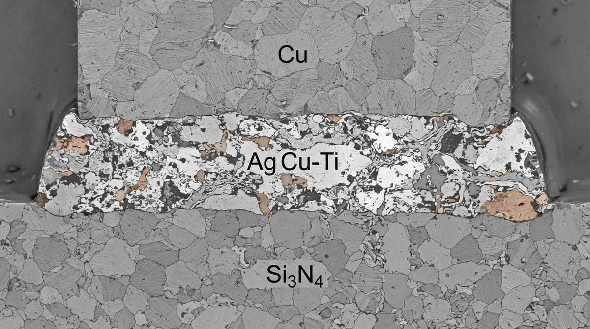
Four processes dominate. Each suits a different copper range, substrate material, and production volume.
Direct Bond Copper (DBC)
DBC uses a controlled-atmosphere furnace to bond a pre-rolled copper foil to an oxide ceramic (usually Al₂O₃ 96 % or AlN with an oxide interlayer). The bond forms a eutectic Cu–Cu₂O layer at roughly 1 065 °C. Standard foil thicknesses are 127 µm (5 mil), 200 µm, and 300 µm (12 mil). DBC is the workhorse of IGBT modules, delivering thermal resistance values of 0.1–0.2 K·cm²/W through the ceramic, per Rogers curamik datasheets.
Limitation: DBC cannot bond to Si₃N₄ without an oxide interlayer, and the Cu₂O eutectic restricts peak reflow temperature to about 900 °C. Trace/space on etched DBC is typically ≥250 µm at 300 µm copper due to etch undercut.
Active Metal Brazing (AMB)
AMB uses a titanium-containing braze alloy (commonly AgCuTi) to bond copper foil to any ceramic surface, including Si₃N₄ and AlN, at 800–900 °C in vacuum. Copper thickness ranges from 200 µm to 800 µm. The braze layer creates a chemical bond rather than an oxide eutectic, so adhesion and thermal-cycle reliability are superior. Kyocera reports >3 000 cycles (–40 °C / +150 °C) on AMB Si₃N₄ without delamination.
AMB costs 2–5× more than DBC per substrate, driven by the vacuum furnace step and silver-bearing braze foil. It is justified in traction inverters, SiC modules, and other applications where Si₃N₄’s fracture toughness (6–7 MPa·√m per CeramTec data) prevents substrate cracking under thick-copper stress.
Electroplated Copper Build-Up
Starting from a sputtered or DPC seed layer (typically Ti/Cu, 0.1–0.5 µm), copper is electroplated to the target thickness. This method allows finer features than DBC—down to 50–75 µm line/space at 100 µm copper—because it avoids foil etching. Production rates are slower: plating 100 µm at 1.5 µm/min takes over an hour per panel. For details on achievable tolerances, see copper plating capabilities and tolerances.
Adhesion depends entirely on the seed layer quality. Peel strength for sputtered Ti/Cu on 96 % alumina typically reaches 2–4 N/mm, adequate for most applications but below DBC’s oxide-bonded values. Thermal cycling performance must be qualified for each thickness and substrate combination.
Thick-Film Printed Copper
Screen-printed copper paste, fired at 850–950 °C in nitrogen, produces layers of 15–25 µm per pass. Two or three passes can yield 50–75 µm, but adhesion degrades and line definition blurs with each pass. This route suits moderate-current circuits where DBC’s minimum feature size is too coarse. Consult thick-film copper thickness and capabilities for printable ranges and paste options.
Thick Copper Ceramic PCB: Property Comparison
| Parameter | DBC | AMB | Electroplated | Thick-Film (multi-pass) |
|---|---|---|---|---|
| Copper thickness range | 127–300 µm | 200–800 µm | 10–200 µm | 15–100 µm |
| Substrate materials | Al₂O₃, AlN | Al₂O₃, AlN, Si₃N₄ | Al₂O₃, AlN | Al₂O₃, AlN |
| Peel strength (N/mm) | 4–6 | 5–8 | 2–4 | 1.5–3 |
| Min trace / space | 250–400 µm | 300–500 µm | 50–150 µm | 150–250 µm |
| Thermal cycle reliability (–40/+150 °C) | ~1 000 cycles | >3 000 cycles | 500–1 500 cycles | 500–1 000 cycles |
| Relative cost per substrate | 1× | 2–5× | 1.5–3× | 0.5–1× |
Typical values for commercially available material, for comparison only. Confirm against the datasheet for your specific grade. DBC and AMB data referenced from Rogers curamik and Kyocera published datasheets; plating and thick-film values from industry norms.
Current Capacity: A Worked Example
A 300 µm copper trace on an AlN DBC substrate, 5 mm wide and 20 mm long, carries DC current with the following approximate resistance:
R = ρ × L / (W × t)
R = 1.72 × 10⁻⁸ Ω·m × 0.020 m / (0.005 m × 0.0003 m)
R = 0.229 mΩ
At 50 A DC, I²R loss = 50² × 0.229 × 10⁻³ = 0.57 W. That heat spreads through the AlN substrate (170–200 W/mK) into the heatsink. On an FR-4 board, the same 50 A would require either a much wider trace or a bus bar, and the substrate itself would add significant thermal resistance.
This is why thick copper ceramic substrates dominate in IGBT half-bridge modules, SiC gate drivers, and LED COB arrays above 50 W. The copper handles the current; the ceramic handles the heat and the voltage isolation (typically >10 kV/mm for 96 % Al₂O₃ per ASTM D149).
Design Considerations for Heavy Copper on Ceramic
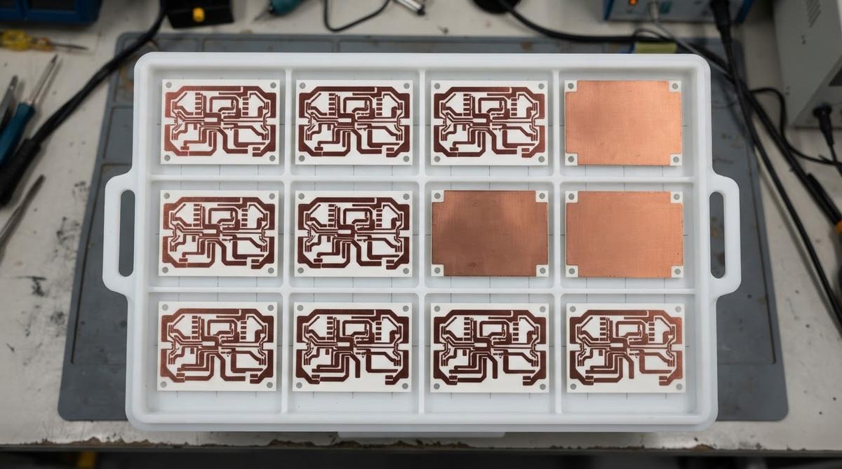
CTE Mismatch Stress
Copper expands 2–4× faster than ceramic. At 300 µm copper on 0.38 mm AlN, the bimetallic stress during soldering or thermal cycling can bow the substrate or, in extreme cases, crack it. Symmetrical metallization (copper on both sides, equal thickness) is standard practice to balance stress. Si₃N₄ substrates tolerate higher stress thanks to fracture toughness roughly 3× that of Al₂O₃.
Trace Resolution vs. Copper Thickness
Thicker copper means wider minimum features. If your design requires traces below 150 µm, electroplating or thin-film deposition is the practical choice. Review thin-film ceramic design rules for feature limits at lower copper thicknesses. For thick-film routing constraints at moderate copper, see the thick-film ceramic design rule reference.
Via Integration
DBC and AMB substrates are typically single-layer. Vias through the ceramic require laser or mechanical drilling before metallization. Filling those vias with copper paste or plated copper adds process steps and cost. For multi-layer builds or thermal via arrays, understand the via filling processes available for ceramic PCBs.
When Thick Copper Ceramic Is Not the Right Choice
Low-current signal boards. If peak current stays below 2 A and thermal density is moderate, standard thin-film or thick-film copper (5–25 µm) on alumina is simpler and cheaper. DBC adds cost with no benefit.
High layer count. DBC and AMB are inherently single- or double-sided. If you need four or more routing layers, LTCC with co-fired conductors or a hybrid organic-ceramic stackup is more practical.
Tight budgets at high volume. For consumer power electronics where cost per unit matters more than thermal-cycle life, aluminum-core MCPCBs (metal-core PCBs) with 2–4 oz copper deliver adequate performance at a fraction of ceramic substrate cost.
Flexible or conformal shapes. Ceramic is brittle. If the assembly must flex, bend, or conform to a curved surface, polyimide flex with heavy copper is the better path.
Frequently Asked Questions
How thick can copper be on a ceramic PCB?
AMB can bond copper foil up to 800 µm (roughly 31 mil) to Si₃N₄ or AlN substrates. DBC reaches 300 µm. Electroplating is practical to about 200 µm. Beyond 800 µm, direct soldering of copper bus bars to the substrate is more common than bonded foil.
Does thick copper crack the ceramic substrate?
It can, especially on Al₂O₃. The CTE mismatch between copper (17 ppm/K) and alumina (6–8 ppm/K) generates tensile stress during cooling. Symmetrical copper on both faces, reduced copper area ratios, and choosing Si₃N₄ (fracture toughness 6–7 MPa·√m) all reduce cracking risk. Finite-element stress simulation before committing to a design is standard practice.
Is DBC the same as thick copper ceramic?
DBC is one method of achieving thick copper on ceramic, but not the only one. AMB, electroplating, and multi-pass thick-film printing also produce heavy copper layers. DBC specifically refers to the Cu₂O eutectic bonding process at ~1 065 °C.
Can I plate additional copper on top of a DBC substrate?
Yes. Some designs start with a 127 µm DBC foil and electroplate an additional 50–100 µm in select areas to boost local current capacity. The plated copper must be masked and the substrate must be cleaned to ensure adhesion. This hybrid approach adds process steps but allows variable copper thickness on one board.
What surface finishes work on thick copper ceramic PCBs?
ENIG, ENEPIG, immersion silver, and bare copper with OSP are all used. For wire bonding pads, electroless nickel / electroless palladium / immersion gold (ENEPIG) is preferred. For soldering power devices, bare copper or immersion silver provides the lowest thermal interface resistance. The finish choice depends on the die-attach method, not the copper thickness.
What is the maximum operating temperature for a thick copper ceramic PCB?
The ceramic substrate itself can withstand well above 800 °C, but the practical limit is set by the copper-ceramic bond and the solder or die-attach material. DBC bonds are stable to about 400 °C; AMB braze joints tolerate up to roughly 600 °C. For a full discussion of thermal limits, see ceramic PCB maximum temperature ratings.
Next Step
If your design calls for copper above 50 µm on a ceramic substrate, the process choice—DBC, AMB, or plated build-up—drives your minimum feature size, cost, and reliability envelope. Prepare your copper thickness requirement, substrate material preference, and expected thermal cycle profile, then request a quote to get specific pricing and lead times for your configuration.