Thick film ceramic PCBs use screen-printed metallic pastes—typically copper, silver, or gold—fired onto a ceramic substrate at 850–1000 °C. Finished conductor thickness usually falls between 10 µm and 50 µm per print-fire cycle, with most production targeting 12–25 µm in a single pass. That range suits resistor networks, hybrid circuits, LED thermal boards, and moderate-current power electronics, but it is not the answer for every project.
Key Takeaways
- Single-pass thick film conductors fire to 10–25 µm; multiple passes can build up to roughly 50 µm.
- Minimum line/space is typically 100–150 µm (4–6 mil), wider than thin film but adequate for most power and sensor layouts.
- Substrate choices include 96% Al₂O₃, 99.6% Al₂O₃, and AlN; each affects paste adhesion, thermal performance, and cost.
- Thick film is less expensive per unit than thin film for runs above a few hundred pieces, but cannot match thin film’s sub-25 µm features.
- Thickness tolerance is typically ±3–5 µm on a single print, governed by screen mesh, paste rheology, and firing profile.
How Thick Film Conductors Are Made
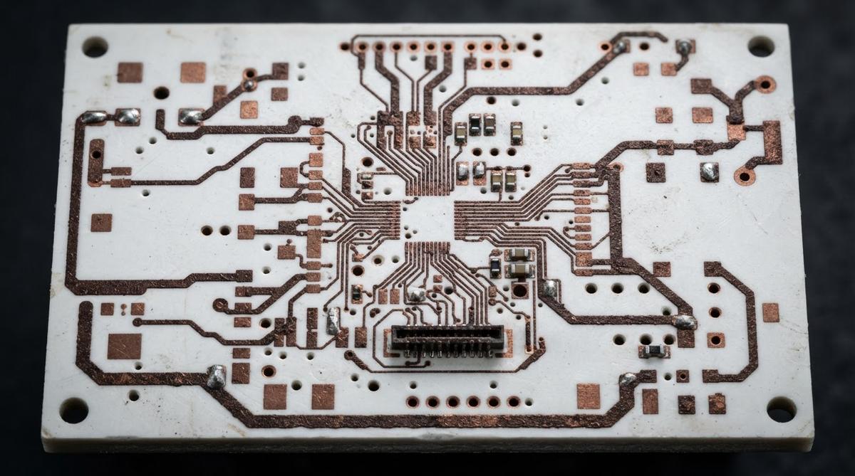
A stainless-steel mesh screen—commonly 200–325 mesh—transfers a metallic paste onto a green or pre-fired ceramic substrate. After printing, the board dries at 100–150 °C, then fires in a belt furnace at 850–1000 °C (for copper paste in a nitrogen atmosphere, or silver/gold in air). During firing, organic binders burn off and glass frit in the paste bonds the metal particles to the ceramic surface.
Each print-fire cycle adds roughly 10–25 µm of conductor. If a design demands thicker copper—say 40–50 µm for higher current—the cycle repeats. Registration between passes is typically ±25 µm, so traces designed for multi-pass buildup should carry extra width margin. For detailed spacing and width rules, see the design rules for thick film ceramic boards.
Achievable Thickness Ranges and Tolerances
| Parameter | Typical Range | Unit | Condition / Notes |
|---|---|---|---|
| Conductor thickness (single pass) | 10–25 | µm | After firing; varies with paste and mesh count |
| Conductor thickness (multi-pass) | 25–50 | µm | 2–3 print-fire cycles |
| Thickness tolerance | ±3–5 | µm | Single print; tighter with finer mesh |
| Min line width | 100–150 | µm | Dependent on mesh count and paste viscosity |
| Min space | 100–150 | µm | Same factors as line width |
| Sheet resistance (Cu, 20 µm fired) | 2–5 | mΩ/□ | Measured at 25 °C; per paste vendor datasheet |
| Adhesion (Cu on 96% Al₂O₃) | 15–30 | N/mm² | Pull test per ASTM F1842 |
Typical values for commercially available materials, for comparison only. Confirm against the datasheet for your specific grade.
Substrate Options for Thick Film
The substrate determines thermal conductivity, dielectric strength, and paste compatibility. Three substrates cover the vast majority of thick film production:
96% alumina (Al₂O₃) is the workhorse: 24–28 W/mK thermal conductivity (at 20 °C, per CoorsTek ADS-996 datasheet), low cost, and well-characterised paste adhesion. Most hybrid circuits, resistor networks, and LED boards use it. See the 96% alumina thick film substrate page for available sizes.
99.6% alumina pushes thermal conductivity to 28–35 W/mK and improves surface finish (Ra < 0.3 µm typical vs. 0.4–0.8 µm for 96%). The smoother surface helps with finer screen prints. It costs roughly 1.5–2× more than 96% alumina.
Aluminum nitride (AlN) delivers 170–200 W/mK, making it the choice for power semiconductors and high-flux LEDs. Paste chemistry must be adjusted—standard glass-frit copper pastes designed for alumina do not bond well to AlN without a compatible adhesion layer or specialised AlN-rated paste. For AlN-specific product details, see the AlN thick film substrate listing.
Thick Film vs. Thin Film: Where the Line Falls
The two processes overlap in application but differ sharply in resolution and cost structure. Thin film sputters or evaporates metal in vacuum, then etches photolithographically. Thick film screen-prints and fires. The table below draws the practical boundary.
| Parameter | Thick Film | Thin Film | Unit |
|---|---|---|---|
| Conductor thickness | 10–50 | 0.5–20 | µm |
| Min line/space | 100–150 | 10–25 | µm |
| Thickness tolerance | ±3–5 | ±0.5–1 | µm |
| Tooling cost | Low (screens) | Higher (masks, vacuum) | — |
| Unit cost at 500 pcs | Lower | Higher | — |
| Best for | Power, LED, resistor networks | RF, MMIC, precision sensors | — |
If your layout has features below 100 µm or needs sub-micron thickness control, thin film ceramic capabilities are worth evaluating. If your traces are 150 µm or wider and your volumes exceed a few hundred boards, thick film almost always wins on cost.
Worked Example: Current Capacity of a 20 µm Thick Film Copper Trace
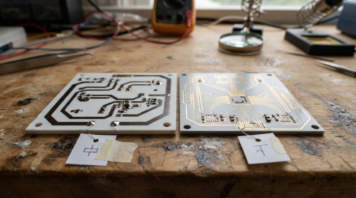
Assume a 500 µm wide, 20 µm thick copper trace on 96% alumina. Cross-sectional area = 0.5 mm × 0.02 mm = 0.01 mm² (≈ 7850 circular mils). Using the IPC-2152 approach for external conductors with a 40 °C temperature rise, a trace this size can carry roughly 1.5–2.0 A in still air. On a ceramic substrate, the superior heat spreading compared to FR-4 pushes the practical limit toward the upper end—but always validate with your own thermal model, because the ceramic’s thermal conductivity helps only if the substrate is properly heat-sunk.
If 2 A is not enough, options include widening the trace, adding a second print pass to reach 40 µm (doubling the cross section), or switching to a DBC (direct bond copper) process that provides 300 µm copper. Thick film is not a high-current bus-bar technology.
Layout Considerations Specific to Thick Film
Screen printing introduces constraints that etched-foil processes do not. Paste tends to slump before firing, so sharp inside corners round off. Design inner radii ≥ 0.1 mm. Pad-to-trace transitions should taper rather than step abruptly; a 45° neck-down reduces print defects. For a full checklist, refer to the thick film layout guidelines.
Via fills in thick film are done with the same paste, screen-printed into laser-drilled or punched holes. Fill quality depends on hole diameter and substrate thickness; aspect ratios above 1:1 become difficult to fill without voids. Typical via diameters range from 0.15 mm to 0.5 mm.
When Not to Use Thick Film Ceramic
Fine-pitch RF or MMIC circuits. If you need 25 µm lines or tighter, thick film cannot resolve them. Use thin film on the same ceramic substrate instead.
High-current bus bars (> 5 A per trace). At 50 µm max copper, thick film traces must be very wide to carry significant current. DBC or AMB (active metal brazing) processes bond 150–500 µm copper foil directly and handle tens of amps per trace.
Cost-sensitive high-volume consumer electronics. If your operating temperature stays below 130 °C and thermal demands are modest, FR-4 or metal-core PCB (MCPCB) will be a fraction of the price.
Tight impedance control. Thick film’s ±3–5 µm thickness variation makes controlled-impedance lines harder to hold than with thin film’s ±0.5–1 µm tolerance. If your RF line impedance budget is ±2 Ω, thin film is the safer bet.
Frequently Asked Questions
Can thick film ceramic handle lead-free soldering?
Yes. Fired thick film metallisation on alumina withstands peak reflow temperatures of 260 °C (per IPC J-STD-020) without delamination. The ceramic substrate itself is stable well above 300 °C, so the limiting factor is paste adhesion and solder joint reliability, not the substrate.
What surface finishes work on thick film ceramic?
Common finishes include electroless nickel / immersion gold (ENIG), electrolytic gold plating, and bare fired copper or silver (with an anti-tarnish coating). Gold is preferred for wire bonding; ENIG suits standard SMT soldering. The choice depends on your assembly method and storage conditions.
Is thick film silver cheaper than thick film copper?
Silver paste fires in air, eliminating the need for a nitrogen atmosphere furnace. That simplifies processing and can reduce cost per board by 10–20%. However, silver is susceptible to electromigration at high humidity and DC bias, so copper or gold is preferred for reliability-critical circuits. More on silver metallisation is available on the silver metallized ceramic page.
How many layers can a thick film ceramic board have?
Thick film is inherently a surface process—conductors are printed on the top, bottom, or both sides of a single substrate. For true multilayer builds (three or more conductor layers), LTCC (low-temperature co-fired ceramic) or sequential thick film with dielectric interlayers is used. Sequential builds are limited to 3–5 layers before yield drops significantly.
Does thick film work on substrates thinner than 0.5 mm?
Yes, but handling fragility increases. Substrates down to 0.25 mm are printable if the production line uses vacuum chucks and careful handling fixtures. Breakage rates rise below 0.38 mm, so expect yield-related cost increases on very thin substrates.