DPC (Direct Plated Copper) is a metallization process that deposits copper onto a fired ceramic substrate by sputtering a seed layer, then building thickness through electroplating and photolithographic patterning. Following proven DPC direct plated copper design rules is essential because this process produces the finest trace/space of any ceramic PCB metallization method—typically 30–75 µm line/space on production panels. The rules below define what is manufacturable and what will cause yield loss.
Key Takeaways
- Minimum trace/space for production DPC is 30/30 µm on Al₂O₃ 96% substrates; 50/50 µm is a safer target for new designs.
- Copper thickness ranges from 1 µm to roughly 50 µm, with most power and RF designs landing between 5 µm and 20 µm.
- Via diameters start at approximately 100 µm (laser-drilled); aspect ratio should stay below 1:1 for reliable plating fill.
- Substrate surface roughness directly affects achievable line definition—Ra ≤ 0.3 µm is recommended for traces below 50 µm.
- DPC is a post-fire process: it works only on pre-sintered substrates (Al₂O₃, AlN, Si₃N₄, ZrO₂), not with co-fired ceramics.
How DPC Metallization Works (Short Version)
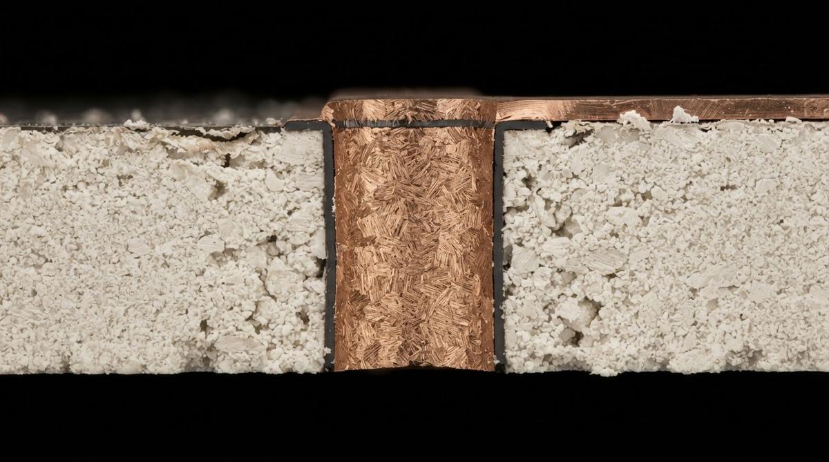
A titanium or chromium adhesion layer (typically 20–50 nm) is sputtered onto the polished ceramic surface, followed by a copper seed layer (100–300 nm). Photoresist is applied and patterned with UV lithography. Copper is then electroplated into the open areas to the target thickness. After resist strip and seed-layer etch, the result is a high-purity copper circuit bonded directly to the ceramic. For more detail on the plating step, see copper plating capabilities and tolerances.
Because the patterning is photolithographic rather than screen-printed, DPC achieves resolution comparable to thin-film processes but with much thicker copper. This makes it the preferred method for power electronics, high-frequency hybrids, and LED thermal substrates where both fine features and current-carrying capacity matter.
DPC Direct Plated Copper Design Rules: Minimum Trace and Space
The practical minimum depends on copper thickness. Thicker plating requires wider spaces to avoid bridging during electroplating and to survive the seed-layer etch without undercutting the traces. These DPC direct plated copper design rules for trace geometry are the single most common source of first-spin yield loss.
| Copper Thickness (µm) | Min Trace Width (µm) | Min Space (µm) | Notes |
|---|---|---|---|
| 1–5 | 30 | 30 | Requires Ra ≤ 0.3 µm substrate |
| 5–15 | 50 | 50 | Standard production target |
| 15–30 | 75 | 75 | Etch factor limits resolution |
| 30–50 | 100 | 100 | Approaching DBC territory |
Typical values for production DPC processes. Confirm with your fabricator for your specific copper thickness and substrate combination.
A common mistake is specifying 30 µm traces with 20 µm copper. The etch undercut alone can consume 5–10 µm per side, leaving a trace that is electrically narrower than drawn. Design to the table above, or ask your fabricator for their etch compensation rules.
Copper Thickness Selection
DPC copper thickness is not arbitrary—it drives trace resolution, current capacity, thermal spreading, and cost. Thicker copper means longer plating time and higher material cost. Choosing the right thickness is one of the most impactful DPC direct plated copper design rules to get right early.
Worked example: A 200 µm wide trace carrying 2 A continuous on a 10 µm thick DPC layer. Cross-sectional area = 200 × 10 = 2,000 µm² = 2 × 10⁻³ mm². Using copper resistivity of 1.72 × 10⁻⁸ Ω·m at 20 °C, resistance per mm of trace ≈ 8.6 mΩ/mm. For a 10 mm trace run, R = 86 mΩ, and I²R loss = 0.34 W. If that loss is unacceptable, increase copper to 20 µm (halving resistance) or widen the trace.
For RF applications where skin depth matters (skin depth in copper at 10 GHz ≈ 0.66 µm per ASTM B193), copper thicker than 3–5 µm adds mass but not signal performance. Match copper thickness to your operating frequency.
Via Design Rules
Vias in DPC ceramic boards are laser-drilled into the fired substrate before metallization. The ceramic is already sintered, so mechanical drilling is impractical for holes below 200 µm.
- Minimum via diameter: 100 µm (laser-drilled, CO₂ or UV laser depending on substrate).
- Aspect ratio: Keep below 1:1 (depth:diameter) for reliable copper plating fill. A 0.25 mm thick substrate needs vias ≥ 250 µm diameter for fully filled vias.
- Via-to-trace clearance: ≥ 75 µm from via pad edge to nearest trace edge.
- Via pad annular ring: ≥ 50 µm beyond the drilled hole on each side.
Thermal vias in DPC boards are commonly arrayed under power devices. For effective thermal paths, use filled and plated-over vias rather than open vias, which trap solder and create voids during die attach.
Substrate Selection and Surface Preparation
DPC works on any pre-sintered ceramic that accepts sputtered adhesion layers. The most common substrates are Al₂O₃ 96%, Al₂O₃ 99.6%, and AlN. Si₃N₄ is used where mechanical toughness matters, though its higher cost and lower thermal conductivity (60–90 W/mK vs. 170–200 W/mK for AlN, per CoorsTek and Kyocera datasheets) make it a niche choice.
Surface roughness is the single biggest variable in DPC yield. A substrate with Ra > 0.5 µm will cause seed-layer discontinuities and trace edge roughness. For traces ≤ 50 µm, specify lapped and polished substrates with Ra ≤ 0.3 µm. As-fired alumina (Ra typically 0.4–0.8 µm) is adequate for traces ≥ 100 µm but marginal for fine-line work.
Dimensional and Position Tolerances
| Parameter | Typical Tolerance | Condition |
|---|---|---|
| Trace width | ±5 µm | On polished substrate, Cu ≤ 10 µm |
| Trace position | ±10 µm | Relative to substrate edge datum |
| Layer-to-layer registration | ±15 µm | Double-sided DPC |
| Via position | ±15 µm | Laser-drilled, referenced to metallization |
| Substrate outline | ±50 µm | Laser-scribed and snapped |
Representative production tolerances. Tighter values are possible at higher cost and lower yield.
DPC vs. Other Ceramic Metallization Methods
Understanding where DPC direct plated copper design rules differ from other metallization approaches helps you pick the right process. The table below shows where each method sits.
| Parameter | DPC | Thin Film | Thick Film | DBC |
|---|---|---|---|---|
| Min trace/space | 30/30 µm | 10/10 µm | 100/100 µm | 200/200 µm |
| Copper thickness | 1–50 µm | 0.1–5 µm | 10–15 µm (paste) | 127–500 µm |
| Adhesion strength | High (sputtered Ti/Cu) | High | Moderate (glass frit bond) | Very high (oxide bond) |
| Current capacity | Moderate–high | Low | Moderate | Very high |
| Relative cost | Medium–high | High | Low–medium | Medium |
Indicative comparison. Values vary by fabricator.
If your design needs traces below 30 µm, look at thin-film ceramic design rules. If your traces are all above 100 µm and copper needs exceed 50 µm, DBC or AMB is a better fit. For cost-sensitive designs with ≥ 100 µm features, thick-film design rules apply.
When NOT to Use DPC
High-current power modules (>50 A per trace): DPC copper tops out around 50 µm. DBC (300 µm copper) or AMB handles these currents without exotic trace widths.
Cost-driven consumer products: If your trace/space is 150 µm or wider and the substrate is standard alumina, thick-film screen printing costs 30–50% less than DPC for equivalent functionality.
Multilayer structures with many internal layers: DPC is inherently a surface-metallization process. For 4+ layer ceramic boards, HTCC or LTCC co-firing is the standard approach.
Flexible or large-area boards: Ceramic substrates are brittle and typically limited to panel sizes under 150 × 150 mm. FR-4 or metal-core PCBs serve large-area thermal designs more economically.
Frequently Asked Questions
Can DPC handle double-sided circuits?
Yes. Both sides of the ceramic substrate are sputtered and plated independently, with through-vias providing electrical connection. Layer-to-layer registration is typically ±15 µm. Double-sided DPC adds one full process cycle, roughly doubling metallization cost.
What surface finishes work on DPC copper?
ENIG, ENEPIG, immersion silver, and OSP are all compatible with DPC copper. ENIG (3–5 µm Ni / 0.05–0.1 µm Au) is the most common for wire bonding and soldering. Electrolytic gold up to 1–2 µm is used for high-reliability wire-bond pads.
Does DPC work on aluminum nitride?
Yes, and AlN is one of the most common DPC substrates for power and LED applications. The sputtered Ti adhesion layer bonds well to AlN. Note that AlN requires careful handling—it reacts with moisture over time, so passivation or hermetic packaging is recommended for long-term reliability.
How does DPC adhesion compare to DBC?
DBC bonds copper through a high-temperature Cu-O eutectic, producing peel strengths of 8–12 N/mm (per Rogers curamik datasheets). DPC sputtered adhesion layers achieve 4–8 N/mm, which is adequate for most soldering and wire bonding but lower than DBC. Thermal cycling reliability of DPC is generally comparable to DBC for copper thicknesses below 30 µm.
What file format should I submit for DPC fabrication?
Gerber RS-274X or ODB++ with a separate drill file for via locations. Include a fabrication drawing specifying copper thickness, substrate material, surface finish, and any critical tolerances. DXF is accepted for substrate outlines and scoring lines.
Next Step
Review the detailed DPC layout guidelines for pad geometry, solder mask rules, and panelization. When your design files are ready, request a quote to confirm manufacturability and lead time.