DPC (direct plated copper) achieves fine-line metallization on ceramic substrates by sputtering a thin adhesion/seed layer onto fired ceramic, then electroplating copper to the target thickness through a photoresist pattern. Following proven DPC direct plated copper layout guidelines is essential because typical DPC processes resolve 30–75 µm (1.2–3 mil) trace and space on Al₂O₃ or AlN substrates, with copper thickness from roughly 5 µm up to about 100 µm. The guidelines below will help you lay out a DPC circuit that manufactures reliably on the first run.
Key Takeaways
- Minimum trace/space for DPC is typically 30–50 µm (1.2–2.0 mil) on polished substrates; production-safe designs target ≥ 50 µm.
- Copper thickness ranges from about 5 µm to 100 µm; thicker copper requires wider trace/space to maintain etch resolution.
- Pad-to-edge clearance should be ≥ 200 µm to avoid chipping during laser scribing and panel breakout.
- DPC bond strength depends on the sputtered seed layer; consult your fabricator’s adhesion spec (typical peel strength ≥ 6 N/mm per IPC-TM-650 2.4.8).
- Thermal vias are not native to DPC on monolithic ceramic; through-holes require laser or mechanical drilling before metallization.
How DPC Direct Plated Copper Layout Guidelines Relate to the Process
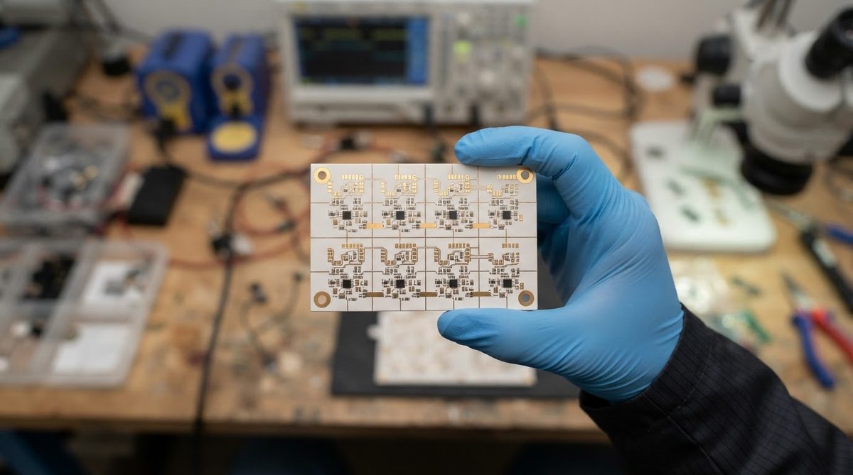
DPC starts with a fired, lapped ceramic substrate. A thin adhesion layer (typically Ti or Cr, 20–100 nm) and a copper seed layer (200–500 nm) are deposited by magnetron sputtering across the full panel. Photoresist is applied, exposed, and developed to define the circuit pattern. Copper is then electroplated into the open areas to the specified thickness. After stripping the resist, a brief differential etch removes the exposed seed layer between traces.
This sequence means your minimum feature size is governed by three things: photoresist resolution, copper plating uniformity, and the seed-layer etch step. Thicker copper requires longer plating, which causes more lateral growth at trace edges, so trace/space minimums increase with copper thickness. Understanding this relationship is the single most important rule in any set of DPC direct plated copper layout guidelines. For more on the seed layer itself, see the page on sputtered seed layers in DPC metallization.
Trace and Space Rules by Copper Thickness
The table below gives conservative, production-proven minimums that form the backbone of reliable DPC direct plated copper layout guidelines. Tighter features may be achievable on polished substrates (Ra < 0.1 µm) with optimised resist processing, but confirm with your fabricator before committing.
| Copper Thickness (µm) | Min Trace Width (µm) | Min Space (µm) | Notes |
|---|---|---|---|
| 5–10 | 30 | 30 | Requires polished substrate, fine-line resist |
| 10–30 | 50 | 50 | Most common for signal and sensor circuits |
| 30–50 | 75 | 75 | Power routing, moderate current |
| 50–100 | 100 | 100 | High-current pads; approaches thick copper ceramic PCB territory |
Values are typical for commercially available DPC processes on 96% Al₂O₃ and AlN. Confirm against your fabricator’s design rule document for your specific grade and surface finish.
Pad and Land Pattern Design
Die-attach pads on DPC substrates serve double duty: electrical connection and thermal dissipation. A few rules keep both functions reliable.
- Minimum pad size: 150 × 150 µm for wire-bond pads; 300 × 300 µm for solder-attach pads. Smaller pads reduce solder fillet volume and weaken the joint.
- Solder mask clearance: If solder mask (polyimide or screen-printed glass) is used, allow ≥ 50 µm clearance per side between the mask opening and the copper pad edge.
- Thermal pad coverage: For power die, keep the copper pad at least 0.5 mm larger than the die on each side to spread heat into the ceramic. Avoid large unbroken copper planes > 10 × 10 mm without relief patterns; plating uniformity degrades on very large open areas.
- Fiducials: Place at least two fiducials (500 µm diameter circle in copper, with 1 mm clearance ring) for pick-and-place alignment.
Enter your substrate dimensions, copper thickness, and trace geometry to check whether your layout meets standard DPC design rules.
Worked Example: Current-Carrying Capacity of a DPC Trace
Suppose you need to route 2 A continuously on a DPC trace. The substrate is 96% Al₂O₃ (thermal conductivity 24–28 W/m·K at 25 °C per CoorsTek ADS-96R datasheet). Ambient temperature is 25 °C; maximum allowable trace temperature rise is 20 °C.
For a copper trace on ceramic, the dominant cooling path is conduction into the substrate, not convection. A simplified estimate uses the Joule heating equation:
P = I² × R, where R = ρ × L / (W × t).
Copper resistivity ρ at 45 °C ≈ 1.85 × 10⁻⁸ Ω·m. For a 10 mm long trace, 200 µm wide, 30 µm thick:
R = 1.85 × 10⁻⁸ × 0.01 / (200 × 10⁻⁶ × 30 × 10⁻⁶) = 0.031 Ω
P = (2)² × 0.031 = 0.124 W over 10 mm length.
At 0.124 W dissipated into a ceramic substrate with 24 W/m·K conductivity and a 0.635 mm substrate thickness, the temperature rise is modest—well under 5 °C. The trace is safe. If you were routing 10 A, the same cross-section would dissipate 3.1 W over 10 mm, and you would need a significantly wider trace or thicker copper. This is where DPC designs sometimes transition to thick copper on ceramic or DBC processes.
Edge Clearance and Panel Layout
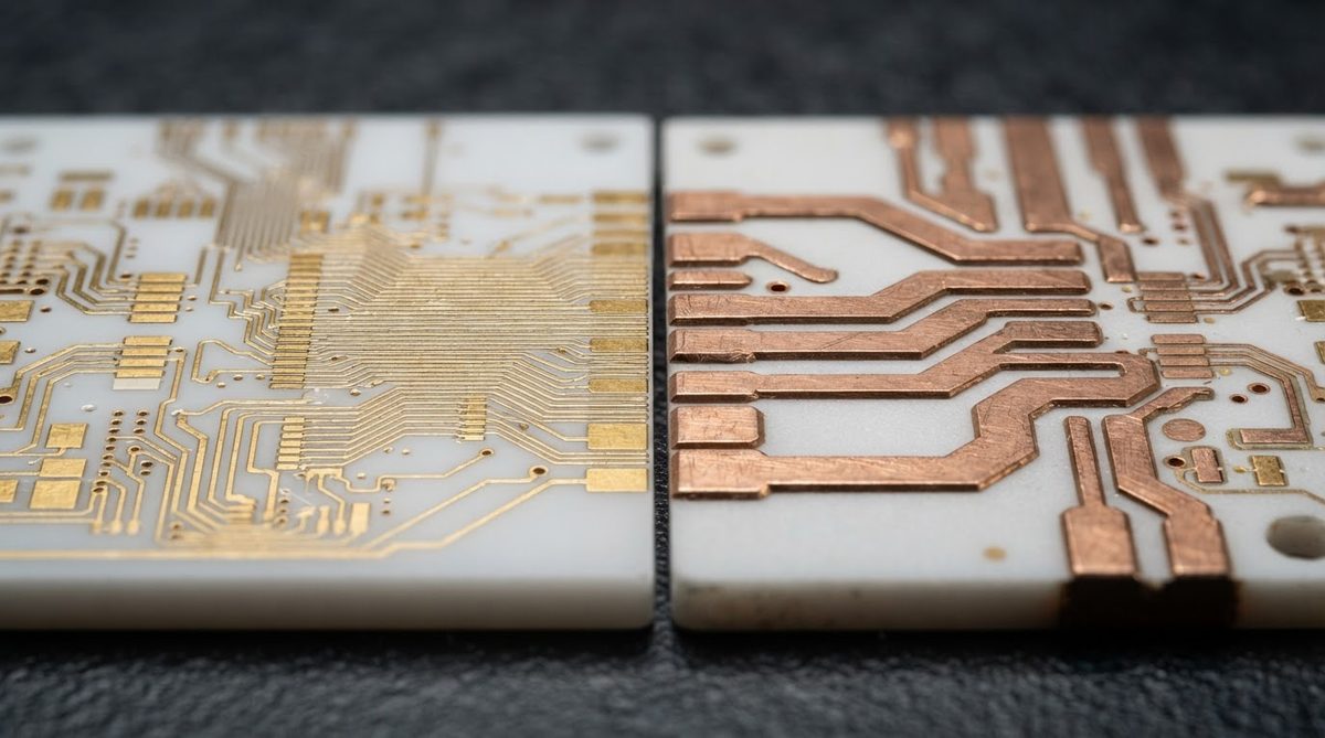
Ceramic substrates are brittle. Copper or solder pads placed too close to the substrate edge risk chipping during singulation. Maintain ≥ 200 µm clearance from any metallization to the substrate edge. For boards singulated by laser scribing, increase this to ≥ 250 µm because the scribe groove can propagate micro-cracks into nearby features.
If your design requires conductors at the board edge—for example, castellation pads for surface-mount modules—review the requirements for edge plating on ceramic PCBs separately, as these use a different metallization sequence.
DPC vs. Other Ceramic Metallization: When to Choose What
Selecting the right metallization process is as important as following DPC direct plated copper layout guidelines. The comparison below shows where DPC fits relative to alternatives.
| Parameter | DPC | Thin Film | Thick Film | HTCC |
|---|---|---|---|---|
| Min trace/space | 30–50 µm | 10–25 µm | 100–125 µm | 100–150 µm |
| Copper thickness | 5–100 µm | 0.5–5 µm (Au, Cu, NiCr) | 8–15 µm (screen print) | 10–25 µm (co-fired W/Mo) |
| Substrate state | Post-fired | Post-fired | Post-fired | Green tape |
| Via capability | Laser-drilled, metallised | Laser-drilled, metallised | Punched, filled | Punched, filled |
| Best for | Power LED, sensors, RF hybrids | Precision resistors, RF filters | Hybrid modules, heaters | Multilayer hermetic packages |
Thin film rules are covered in the thin film ceramic layout guidelines page.
When Not to Use DPC
You need multilayer routing. DPC is inherently a single- or double-sided process. If your circuit needs three or more metal layers with buried vias, HTCC or LTCC co-fired ceramics are the correct choice.
You need copper thicker than ~100 µm. Electroplating beyond 100 µm on a sputtered seed layer becomes slow and expensive, with diminishing edge definition. DBC (direct bond copper) handles 150–500 µm copper on ceramic more economically.
Your budget is tight and tolerances are loose. If 100 µm trace/space is fine and you do not need the adhesion or thermal performance of sputtered copper, thick film screen printing costs less per unit area.
You need sub-25 µm features. Thin film (sputter + etch, no plating) resolves finer lines than DPC. The trade-off is much thinner metallization.
FAQ
Can I use standard Gerber files for a DPC design?
Yes. DPC fabricators accept standard Gerber RS-274X or ODB++ output. Include a fabrication drawing that specifies copper thickness, substrate material, substrate thickness, and surface finish. Call out any critical dimensions separately.
Does DPC copper peel off ceramic substrates?
Properly sputtered adhesion layers (Ti or Cr) yield peel strengths of 6–10 N/mm, which exceeds most wire-bond and solder-joint requirements. Peel failures almost always trace back to contaminated substrates or insufficient seed-layer thickness. Ask your fabricator for peel-test data per IPC-TM-650 method 2.4.8.
What surface finishes can go on top of DPC copper?
Common finishes include electroless nickel / immersion gold (ENIG), electrolytic nickel/gold, and bare copper with OSP. For wire bonding, electrolytic gold ≥ 0.5 µm over nickel is standard. For soldering, ENIG (3–5 µm Ni, 0.05–0.1 µm Au) works well.
Is DPC suitable for RF and microwave circuits?
DPC on AlN or 99.6% Al₂O₃ is used in RF hybrid modules up to several GHz. The sputtered seed layer provides a smooth, low-loss copper surface. For frequencies above ~20 GHz, thin film metallization on polished alumina or quartz generally offers tighter impedance control due to finer line definition.
How do I add vias to a DPC ceramic board?
Vias are laser-drilled (typically CO₂ or UV laser) into the fired ceramic before metallization. The via walls are then metallised during the same sputter-and-plate sequence as the surface traces. Minimum via diameter is typically 100–150 µm, depending on substrate thickness. Aspect ratios above 1:1 become difficult to plate uniformly.