Ceramic substrate polishing brings surface roughness from a typical as-fired Ra of 0.4–0.8 µm down to Ra 0.025–0.05 µm, and in some cases below Ra 0.01 µm. This matters because thin-film sputtered metallization demands a smooth, defect-free surface to achieve sub-25 µm line/space resolution and consistent film adhesion. If your design uses thick-film processes, you likely do not need polishing at all.
Key Takeaways
- As-fired 96% alumina substrates typically measure Ra 0.4–0.8 µm; 99.6% alumina fires smoother at Ra 0.15–0.4 µm (per Kyocera A-493 datasheet).
- Lapping with 9 µm alumina slurry brings roughness to Ra 0.1–0.2 µm; final polishing with 1 µm or finer diamond slurry reaches Ra <0.05 µm.
- Polishing adds 15–30% to bare substrate cost depending on volume, material, and target roughness.
- Thin-film circuits with sputtered or evaporated metals require polished substrates; thick-film screen-printed circuits generally do not.
- Flatness (TTV, total thickness variation) of ≤5 µm across a 50 mm substrate is achievable with precision lapping.
Why Surface Roughness Matters for Ceramic PCBs
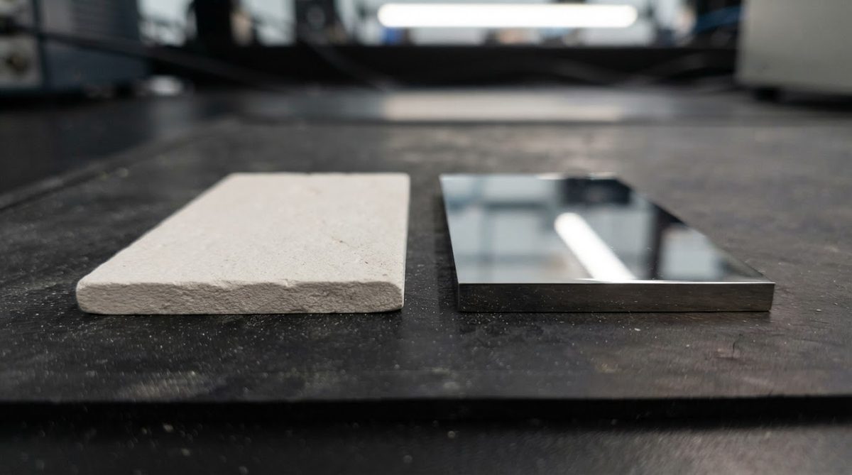
A ceramic substrate’s surface roughness directly affects three things: metallization adhesion, line definition, and high-frequency signal loss. Sputtered thin films—typically Ti/Pt/Au or TiW/Cu stacks—are only tens of nanometres to a few micrometres thick. Surface peaks taller than the film thickness cause discontinuities, open circuits, or weak spots that fail under thermal cycling.
At RF and microwave frequencies, surface roughness also increases conductor loss. The skin depth of copper at 10 GHz is approximately 0.66 µm. If the substrate roughness approaches or exceeds this value, current follows a longer, more resistive path along the surface contour. Polishing the substrate before metallization reduces these losses measurably. For designs following thin-film layout guidelines, a polished substrate is a prerequisite, not an option.
Lapping vs. Polishing: What Each Step Does
The terms are often used interchangeably, but they are distinct operations with different goals.
Lapping is a material-removal step. The substrate is pressed against a rotating cast-iron or composite plate flooded with an abrasive slurry—usually alumina (Al₂O₃) or silicon carbide (SiC) particles in water. The goal is to flatten the substrate, control thickness to tight tolerances (TTV ≤ 5 µm), and reduce roughness to the Ra 0.1–0.2 µm range. Lapping removes 10–200 µm of material per side depending on the starting condition.
Polishing follows lapping. It uses a compliant polyurethane or pitch pad with fine diamond slurry (1 µm, 0.5 µm, or 0.25 µm particle size). Material removal is minimal—typically 1–5 µm. The goal is purely surface quality: reducing Ra below 0.05 µm and eliminating sub-surface damage left by lapping. Some optical-grade applications push to Ra <0.01 µm with colloidal silica final polish.
Typical Abrasive Sequence
| Step | Abrasive | Particle Size | Plate / Pad | Target Ra | Material Removed |
|---|---|---|---|---|---|
| 1 – Rough lap | SiC or Al₂O₃ | 15–25 µm | Cast iron | 0.2–0.4 µm | 50–200 µm |
| 2 – Fine lap | Al₂O₃ | 5–9 µm | Cast iron or composite | 0.1–0.2 µm | 5–20 µm |
| 3 – Rough polish | Diamond | 1–3 µm | Polyurethane pad | 0.03–0.08 µm | 1–5 µm |
| 4 – Final polish | Diamond or colloidal silica | 0.25–0.5 µm | Pitch or soft pad | <0.025 µm | <1 µm |
Typical values for commercially available abrasives and alumina substrates. Confirm against the datasheet for your specific grade. Sequence adapted from Logitech Ltd. ceramic processing application notes.
Not every substrate needs all four steps. A thick-film substrate going through screen printing may only need a single lapping step—or none at all—since the printed paste fills surface irregularities during firing.
Achievable Surface Roughness by Ceramic Material
| Material | As-Fired Ra (µm) | After Lapping Ra (µm) | After Polishing Ra (µm) | Source |
|---|---|---|---|---|
| Al₂O₃ 96% | 0.4–0.8 | 0.1–0.2 | 0.02–0.05 | CoorsTek ADS-996 datasheet |
| Al₂O₃ 99.6% | 0.15–0.4 | 0.05–0.15 | 0.01–0.03 | Kyocera A-493 datasheet |
| AlN | 0.3–0.6 | 0.08–0.15 | 0.015–0.04 | Maruwa AN-230 datasheet |
| Si₃N₄ | 0.2–0.5 | 0.08–0.12 | 0.01–0.03 | CeramTec SN-HP datasheet |
Typical values for commercially available material, for comparison only. Confirm against the datasheet for your specific grade.
Higher-purity alumina polishes smoother because its finer grain structure (1–3 µm grains in 99.6% vs. 5–15 µm in 96%) creates fewer grain pull-out pits during lapping. If your design needs Ra <0.03 µm, start with 99.6% alumina or AlN rather than trying to force 96% alumina to that level.
Worked Example: Thickness Control for a Thin-Film Hybrid
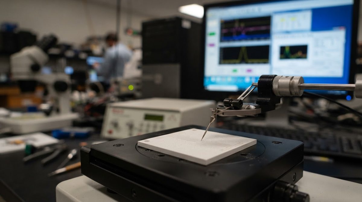
Suppose you need a 50.8 × 50.8 mm alumina substrate at 0.635 mm ± 0.010 mm thickness, with TTV ≤ 5 µm and Ra ≤ 0.05 µm for a sputtered TiW/Cu thin-film circuit.
- Start with an as-fired blank at 0.70 mm nominal (oversize by ~65 µm to allow removal).
- Rough-lap both sides with 15 µm SiC to reach 0.650 mm. This removes ~25 µm per side and brings TTV under 10 µm.
- Fine-lap with 9 µm Al₂O₃ to 0.638 mm. TTV drops below 5 µm. Ra is now ~0.15 µm.
- Polish one side (the metallization face) with 1 µm diamond slurry. Remove ~3 µm. Ra reaches 0.04 µm.
- Final-polish with 0.25 µm diamond. Ra drops below 0.025 µm. Final thickness: 0.635 mm ± 0.005 mm.
Total processing time per substrate on a batch lapping machine: roughly 30–60 minutes depending on equipment and batch size. The ceramic substrate thickness chart lists standard blanks that serve as starting points for this kind of work.
Cost Impact of Polishing
Polishing is a significant cost adder. A rough breakdown for 96% alumina, 50 × 50 mm substrates in a batch of 100:
| Condition | Relative Cost | Typical Use Case |
|---|---|---|
| As-fired (no lapping) | 1.0× | Thick-film, non-critical |
| Lapped (Ra 0.1–0.2 µm) | 1.10–1.15× | Thick-film with tight thickness tolerance |
| Polished (Ra 0.03–0.05 µm) | 1.15–1.25× | Standard thin-film metallization |
| Mirror-polished (Ra <0.01 µm) | 1.25–1.40× | Optical, MEMS, high-frequency thin-film |
Cost multipliers are approximate and vary with volume, material, and vendor. Request a quote for exact pricing.
The cost increase comes from machine time, consumables (diamond slurry is expensive), yield loss from handling thin ceramics, and the metrology needed to verify roughness and flatness. For thin-film ceramic design rules requiring sub-25 µm features, this cost is unavoidable.
When Not to Polish a Ceramic Substrate
Polishing is unnecessary—and a waste of money—in several common scenarios:
- Thick-film circuits. Screen-printed pastes are 10–25 µm thick after firing and conform to the substrate surface. An as-fired substrate with Ra 0.4–0.8 µm works fine. Consult thick-film layout guidelines for surface requirements.
- DBC (direct bond copper) substrates. The copper bonding process uses a eutectic oxide layer that fills minor surface irregularities. Lapping may be needed for flatness, but mirror polishing is not.
- Structural or thermal-only substrates. If the ceramic is a heat spreader or insulator with no fine metallization, surface finish is irrelevant beyond basic cleanliness.
- FR-4 replacement at low frequency. If your operating frequency is below 1 GHz and your traces are wider than 100 µm, a lapped (not polished) surface is sufficient.
Common Defects from Improper Polishing
Sub-surface damage (SSD)
Aggressive lapping with coarse abrasives introduces micro-cracks 5–20 µm below the surface. These are invisible until a sputtered film delaminates during thermal cycling. The fix is a sufficient fine-lapping step before polishing, removing at least 3× the depth of the coarsest abrasive used.
Grain pull-out
In lower-purity alumina (96%), the glassy grain-boundary phase is softer than the alumina grains. Polishing can pluck entire grains from the surface, leaving pits 5–15 µm across. Switching to a softer pad and finer slurry reduces this, but the most reliable fix is specifying 99.6% alumina.
Edge chipping
Ceramic substrates are brittle. Lapping and polishing apply lateral forces that can chip edges, especially on substrates thinner than 0.38 mm. Proper fixturing and controlled pressure (typically 0.5–2 psi) are essential. The sintering process that precedes lapping also affects edge integrity—over-fired substrates are more prone to chipping.
FAQ
Can I skip polishing and use a finer-grain alumina instead?
Partially. A 99.6% alumina substrate fires to Ra 0.15–0.4 µm, which may be adequate for thick-film or some DPC processes. For sputtered thin-film metallization requiring Ra <0.05 µm, polishing is still needed regardless of alumina purity.
Does polishing weaken the substrate mechanically?
Properly polished substrates are actually stronger than as-lapped ones. Polishing removes the sub-surface damage layer introduced by lapping, which acts as a crack initiation zone. Flexural strength per ASTM C1161 often increases 10–20% after a good polish.
How do I verify surface roughness on incoming substrates?
Use a stylus profilometer (contact) or white-light interferometer (non-contact). Specify the measurement standard (ISO 4287 or ASME B46.1), the evaluation length, and the cutoff wavelength in your purchase order. A single Ra number without these parameters is ambiguous.
Is diamond slurry the only option for final polishing?
No. Colloidal silica (SiO₂, 20–50 nm particle size) is widely used for the final step on alumina and AlN. It combines chemical and mechanical action, producing fewer sub-surface defects than diamond alone. It is slower, adding process time, but delivers Ra values below 0.01 µm reliably.
What flatness should I specify for a polished substrate?
For standard thin-film work, a TTV (total thickness variation) of ≤10 µm across the substrate is typical. Precision applications like MEMS or photolithographic patterning may need TTV ≤5 µm or even ≤2 µm. Tighter flatness costs more and requires single-substrate processing rather than batch lapping.