A thermoelectric cooler AlN PCB delivers 170–200 W/mK thermal conductivity at 20 °C — roughly 6–8× higher than the 96% alumina substrates found in commodity Peltier devices — and its CTE of 4.4–4.7 ppm/°C closely matches the 4.0–5.0 ppm/°C range of bismuth telluride (Bi₂Te₃) thermoelectric elements. That combination of high conductivity and CTE alignment makes the thermoelectric cooler AlN PCB the standard choice when a TEC module must deliver maximum ΔT, survive repeated thermal cycling, or both.
Key Takeaways
- AlN substrates conduct heat 6–8× faster than 96% alumina, reducing parasitic thermal resistance between the TEC hot side and the heat sink.
- The CTE mismatch between AlN and Bi₂Te₃ is typically < 1 ppm/°C, compared to 2–3 ppm/°C for 96% alumina, per Kyocera’s published substrate data.
- AlN substrates cost 3–5× more than alumina per unit area, so they are justified only when the application demands high ΔT, fast response, or long cycling life.
- Typical AlN TEC substrates are 0.25–0.64 mm thick, with DPC or thin-film metallization for the conductor pattern.
Why Thermal Conductivity Matters in a Thermoelectric Cooler AlN PCB
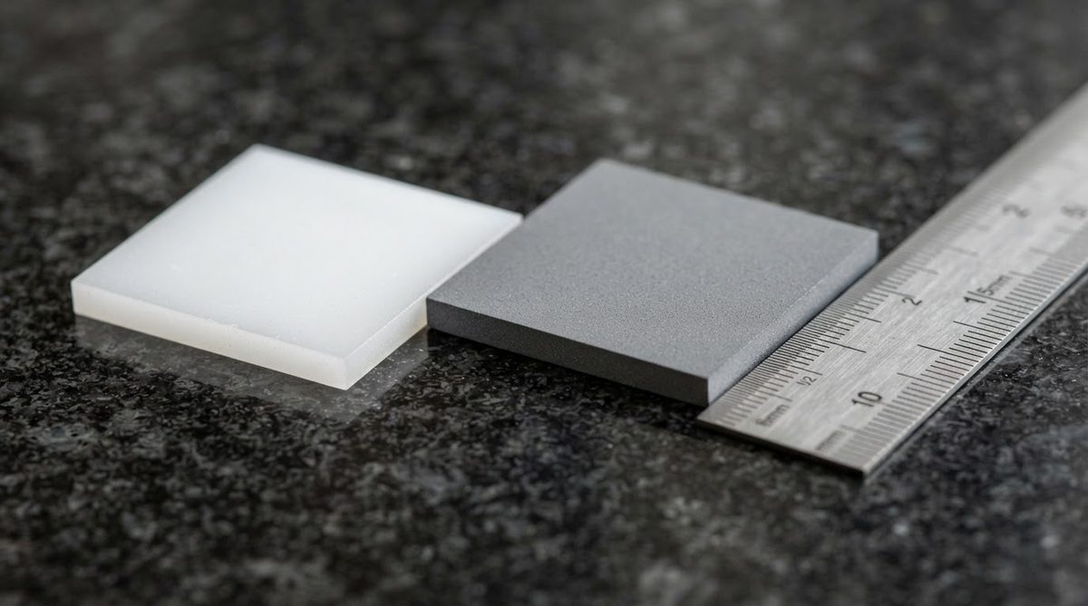
A thermoelectric module is a sandwich: two ceramic substrates bonded to an array of p-type and n-type Bi₂Te₃ pellets through solder. The cold-side substrate absorbs heat from the object being cooled; the hot-side substrate rejects heat into a sink. Any thermal resistance in the substrate directly subtracts from the useful ΔT the module can produce.
Consider a single-stage TEC rated for a maximum ΔT of 70 °C. If the two substrates together contribute 2–3 °C of parasitic temperature drop, that loss is a significant fraction of the total budget. Switching from 96% alumina (24–28 W/mK) to an AlN PCB (170–200 W/mK) cuts the substrate’s thermal resistance by roughly 85%, recovering most of that lost ΔT.
Worked Example: Substrate Thermal Resistance
For a 40 × 40 mm thermoelectric cooler AlN PCB substrate, 0.38 mm thick, carrying 50 W of heat flux:
- 96% Al₂O₃ (25 W/mK): Rth = t / (k × A) = 0.00038 / (25 × 0.0016) = 0.0095 °C/W → ΔT = 50 × 0.0095 = 0.48 °C per substrate, 0.95 °C for both.
- AlN (180 W/mK): Rth = 0.00038 / (180 × 0.0016) = 0.00132 °C/W → ΔT = 50 × 0.00132 = 0.066 °C per substrate, 0.13 °C for both.
The AlN pair saves roughly 0.82 °C of parasitic loss. In a multi-stage cooler targeting cryogenic temperatures, that margin compounds across stages and can determine whether the system reaches its target cold-side temperature.
Enter your substrate dimensions, material, and heat load below to estimate the thermal resistance and temperature drop for your own thermoelectric cooler design.
CTE Matching: Why It Extends TEC Module Life
Every power cycle forces the substrate and the Bi₂Te₃ elements to expand and contract at different rates. The resulting shear stress concentrates at the solder joints. A larger CTE mismatch in ceramic assemblies accelerates solder fatigue and cracks the brittle thermoelectric pellets.
AlN’s CTE of 4.4–4.7 ppm/°C (20–400 °C, per CoorsTek datasheet for ANCeram) sits within the Bi₂Te₃ range of 4.0–5.0 ppm/°C (perpendicular to the c-axis). The resulting mismatch is typically below 1 ppm/°C. By contrast, 96% alumina at 7.1–7.4 ppm/°C creates a 2–3 ppm/°C gap. For modules that must survive > 100,000 thermal cycles — common in telecom laser diode coolers — a thermoelectric cooler AlN PCB is standard practice, as noted in Marlow Industries’ TEC design guides.
AlN vs. Alumina for TEC Substrates: Property Comparison
| Parameter | AlN | 96% Al₂O₃ | Unit | Condition | Source |
|---|---|---|---|---|---|
| Thermal conductivity | 170–200 | 24–28 | W/mK | 20 °C | Kyocera SN series / A-493 datasheets |
| CTE | 4.4–4.7 | 7.1–7.4 | ppm/°C | 20–400 °C | CoorsTek ANCeram / AD-96 datasheets |
| Dielectric strength | 15–17 | 10–15 | kV/mm | 25 °C, ASTM D149 | Maruwa / CoorsTek |
| Flexural strength | 300–350 | 340–380 | MPa | ASTM C1161 | CoorsTek |
| Relative cost (per cm²) | 3–5× | 1× (baseline) | — | 40 × 40 mm, 0.38 mm thick | Industry pricing, 2024 |
Typical values for commercially available material, for comparison only. Confirm against the datasheet for your specific grade.
Metallization Options for Thermoelectric Cooler AlN PCB Designs
TEC modules need a patterned conductor on each substrate to connect the thermoelectric pellets in series electrically and in parallel thermally. The two dominant metallization routes for AlN are:
- Direct Plated Copper (DPC): Sputtered adhesion layer (Ti or TiW) followed by electroplated Cu, typically 10–50 µm. DPC provides fine-line capability (trace/space down to 50 µm) and excellent solder wettability. It suits single-stage and multi-stage coolers for laser diode and detector packaging.
- Active Metal Brazing (AMB): A brazing alloy bonds a thick Cu foil (typically 0.15–0.3 mm) to the AlN. AMB handles higher current loads but offers coarser patterning. It is more common in high-power Peltier modules for industrial cooling.
Both processes can be applied to custom AlN ceramic PCBs tailored to your TEC footprint and pellet count.
Typical Applications
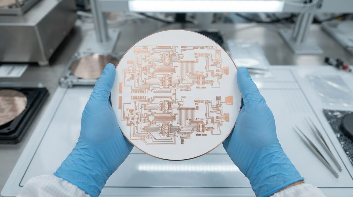
Thermoelectric cooler AlN PCB substrates appear wherever thermal performance justifies the higher cost:
- Telecom laser diode cooling: Wavelength stability demands ±0.01 °C control. AlN substrates enable the fast thermal response and high ΔT needed.
- IR detector and focal-plane array cooling: Multi-stage Peltier coolers reaching −60 °C or below rely on AlN to minimize inter-stage losses.
- PCR and microfluidic thermal cycling: Rapid cycling between 55 °C and 95 °C benefits from AlN’s low thermal mass and high conductivity.
- UV LED thermal management: High-flux UV LED modules on AlN substrates sometimes integrate Peltier cooling to stabilize output wavelength.
When Not to Use AlN for Your TEC
AlN is not always the right call. Standard 96% alumina substrates work well for commodity single-stage TECs where ΔT requirements are modest (≤ 50 °C), cycling life is under 50,000 cycles, and cost pressure is high. Consumer beverage coolers, small desktop climate chambers, and cosmetic device coolers fall into this category. If your 96% alumina substrates already meet your thermal budget, switching to AlN adds cost without measurable benefit.
Similarly, if the dominant thermal resistance in your system is the heat-sink interface or the forced-air path rather than the substrate itself, upgrading the substrate alone will not move the needle. Analyze the full ceramic thermal management stack before specifying AlN.
Design Tips for AlN TEC Substrates
- Keep substrates thin. 0.25–0.38 mm is standard for single-stage TECs. Thinner substrates reduce both thermal resistance and thermal mass, improving transient response.
- Specify surface finish. A lapped or polished surface (Ra < 0.4 µm) improves solder-joint uniformity across the pellet array. Rough surfaces create voids that act as thermal bottlenecks.
- Control metallization thickness. Copper that is too thick increases CTE mismatch at the Cu-AlN interface. For DPC, 20–35 µm is a practical range for most TEC layouts.
- Match solder alloys to your temperature range. High-temperature solders (e.g., AuSn at 280 °C liquidus) are used for the pellet-to-substrate bond in multi-stage coolers so that lower stages can be reflowed without disturbing upper joints.
Sourcing AlN Substrates for TEC Production
For volume TEC manufacturing, wholesale AlN ceramic substrates are available with consistent lot-to-lot thermal conductivity (typically guaranteed ≥ 170 W/mK). Specify incoming inspection for thermal conductivity and surface roughness to avoid field failures from substrate variation.
FAQ
Can I use alumina instead of AlN for a multi-stage TEC?
You can, but performance suffers. Each alumina substrate adds roughly 0.4–0.5 °C of parasitic loss per stage at 50 W heat load (40 × 40 mm, 0.38 mm thick), compared to about 0.07 °C for AlN. In a three-stage cooler, that difference compounds to over 2 °C of lost ΔT, which may prevent the module from reaching its target cold-side temperature.
What surface finish does a thermoelectric cooler AlN PCB need for solder assembly?
A lapped finish with Ra < 0.4 µm is standard. Some high-reliability applications specify Ra < 0.2 µm. The smooth surface ensures uniform solder wetting across all pellet pads, reducing void percentage below the 5% threshold typically required by telecom module specs.
Does AlN outgas in vacuum or hermetic packages?
AlN ceramic itself has negligible outgassing. The metallization layers and any organic residues from processing are the primary outgassing sources. Specify a post-metallization bake (typically 150 °C for 2 hours in vacuum) and verify with residual gas analysis (RGA) per MIL-STD-883 Method 1018 if the TEC will operate in a hermetic enclosure.
How thick should an AlN TEC substrate be?
Most single-stage TECs use 0.25–0.38 mm substrates. Going thinner than 0.25 mm increases breakage risk during pellet soldering. Going thicker than 0.64 mm adds unnecessary thermal resistance and mass. Choose the thinnest substrate your assembly process can handle reliably.
Is AlN compatible with lead-free solder?
Yes. AlN with DPC metallization (Ti/Cu or TiW/Cu) is fully compatible with SAC305 and other lead-free alloys. Wetting angles on properly metallized AlN are comparable to those on alumina. For high-reliability or military TECs, SnPb or AuSn solders remain common due to their established reliability data.