A power supply module AlN PCB conducts heat at 170–200 W/mK (at 20 °C, per Kyocera and Maruwa datasheets), roughly 6–8× better than 96% alumina. For industrial power supply modules dissipating 50–300 W in a small footprint, that difference directly determines whether a MOSFET or SiC transistor stays within its rated junction temperature. AlN also provides dielectric strength above 15 kV/mm, so high-voltage isolation and thermal performance come from the same layer.
Key Takeaways
- AlN substrates offer 170–200 W/mK thermal conductivity at 20 °C, compared with 24–28 W/mK for 96% alumina (source: Kyocera SH-30 and Maruwa HA-200 datasheets).
- A 0.635 mm AlN substrate under a 10 × 10 mm die dissipating 100 W produces roughly 0.035 °C/W conduction resistance—about one-seventh that of the same geometry in 96% alumina.
- AlN’s CTE of 4.4–4.7 ppm/°C closely matches silicon (2.6 ppm/°C) and SiC (4.0 ppm/°C), reducing solder-joint fatigue in power modules that thermal-cycle thousands of times.
- AlN substrates typically cost 3–5× more per unit area than 96% alumina, making them most justified when thermal constraints cannot be met by cheaper alternatives.
Why a Power Supply Module AlN PCB Outperforms Organic Boards
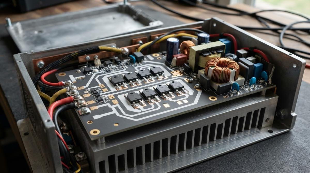
Modern industrial power supplies pack more watts into less board area. A 48 V-to-12 V DC-DC converter in a quarter-brick footprint may dissipate 30–60 W. A three-phase rectifier module for a 10 kW server PSU can concentrate 100+ W across just a few switching devices. FR-4 (0.25 W/mK) and standard metal-core PCB (1–3 W/mK for the dielectric layer) create thermal bottlenecks at these densities.
Ceramic substrates eliminate the organic dielectric entirely. The substrate itself is the insulator and the thermal path. A power supply module AlN PCB is the highest-conductivity electrically insulating option available, which is why it appears in half-bridge modules, PFC stages, and isolated gate drivers where both voltage isolation and heat extraction matter simultaneously.
AlN vs. Alumina: Choosing the Right Ceramic for Power Supply Modules
The table below compares the two most common ceramic substrates used in power electronics. Both work. The question is whether your thermal budget justifies the price difference of a power supply module AlN PCB over an alumina alternative.
| Parameter | AlN (≥ 98%) | Al₂O₃ (96%) | Unit | Condition | Source |
|---|---|---|---|---|---|
| Thermal conductivity | 170–200 | 24–28 | W/mK | 20 °C | Kyocera SH-30 / Maruwa HA-200 |
| Dielectric strength | 15–17 | 10–15 | kV/mm | AC, 1 mm thick | CoorsTek ADS-996 / Kyocera A-476 |
| CTE | 4.4–4.7 | 7.0–7.4 | ppm/°C | 20–400 °C | Maruwa datasheets |
| Flexural strength | 300–400 | 350–380 | MPa | ASTM C1161 | CoorsTek / Kyocera |
| Volume resistivity | > 10¹⁴ | > 10¹⁴ | Ω·cm | 25 °C | Kyocera |
| Relative cost (per cm²) | 3–5× | 1× (baseline) | — | DBC, 0.635 mm | Industry pricing |
Typical values for commercially available material, for comparison only. Confirm against the datasheet for your specific grade.
If your power supply module uses SiC MOSFETs or GaN HEMTs switching at high frequency, the CTE match of AlN becomes as important as its thermal conductivity. AlN substrates for SiC power modules face the same CTE-matching challenge, and the design logic transfers directly to industrial PSU applications.
Worked Example: Thermal Resistance Through a Power Supply Module AlN PCB
Consider a half-bridge module in a 3 kW industrial AC-DC power supply. Two SiC MOSFETs are soldered to a DBC AlN substrate. Each device dissipates 50 W over a 10 mm × 10 mm footprint.
Conduction resistance through the substrate:
Rth = t / (k × A)
- t = 0.635 mm = 0.000635 m
- k = 180 W/mK (mid-range AlN)
- A = 10 mm × 10 mm = 0.0001 m²
Rth,AlN = 0.000635 / (180 × 0.0001) = 0.035 °C/W
Temperature rise through the substrate at 50 W: 0.035 × 50 = 1.8 °C.
Now repeat for 96% alumina (k = 26 W/mK):
Rth,Al₂O₃ = 0.000635 / (26 × 0.0001) = 0.244 °C/W
Temperature rise: 0.244 × 50 = 12.2 °C.
That 10.4 °C difference per device may seem modest in isolation. But add solder layers, copper thickness effects, and a second device on the same substrate, and the margin compounds. In a sealed industrial enclosure with limited airflow, those degrees determine whether you need a fan or can run convection-only.
Enter your own substrate area, thickness, and dissipated power below to estimate junction temperature rise for your specific power supply module AlN PCB design.
Metallization Options for Power Supply Module AlN PCB Substrates
AlN substrates for power supply modules are typically metallized using one of two processes:
DBC (Direct Bond Copper): A copper sheet (typically 0.127–0.3 mm) is bonded directly to the AlN through a controlled oxidation process. DBC handles high current (tens of amps per trace) and provides excellent thermal spreading. It is the standard for power modules above 500 V or 20 A. Copper thickness up to 0.3 mm is common for bus bars and power stages.
DPC (Direct Plated Copper): Sputtered seed layer followed by electroplated copper, typically 1–70 µm. DPC offers finer trace resolution (line/space down to 50 µm or below) and is suited to control circuits, gate drivers, and signal routing on the same ceramic substrate. For power supplies that integrate driver and power stage on one board, a DPC layer handles the logic side.
For high-volume AlN substrate procurement, specifying the metallization process early avoids downstream delays. DBC and DPC require different substrate surface finishes; a polished or lapped AlN substrate improves bond quality for both methods.
Common Power Supply Topologies Using AlN PCBs
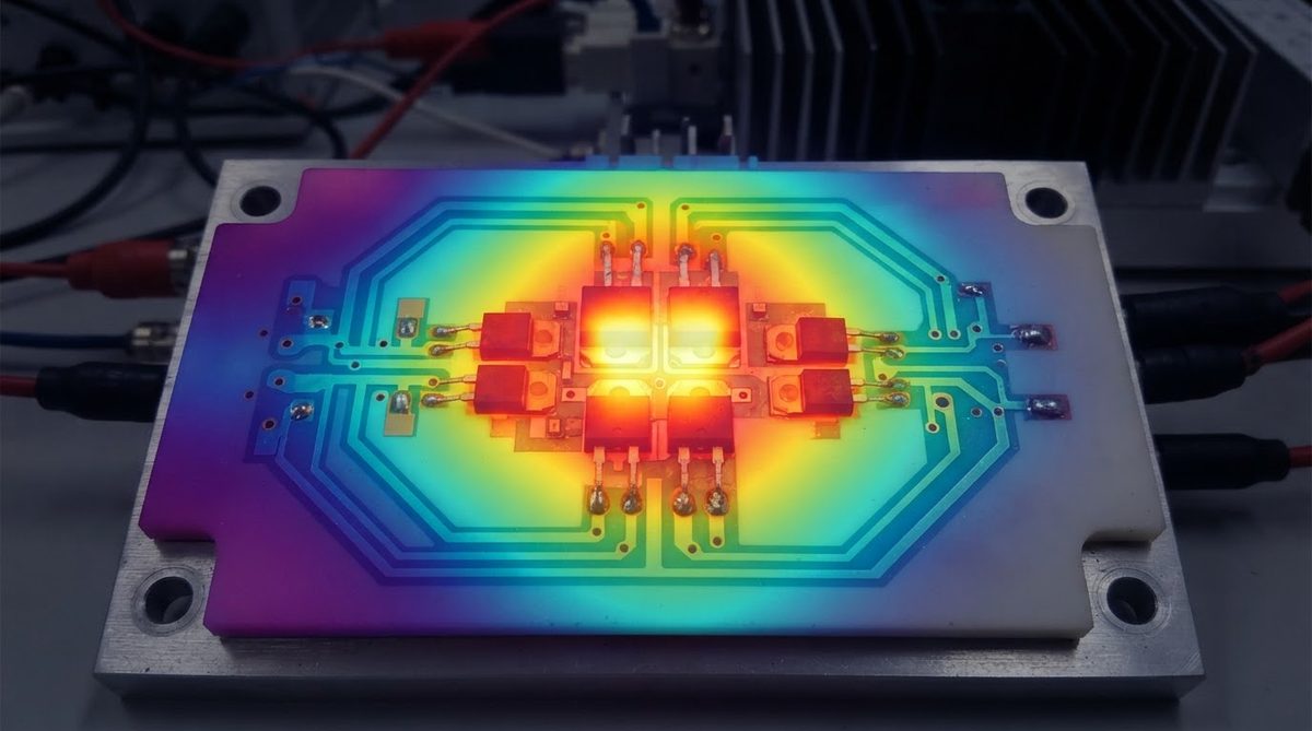
AlN ceramic substrates appear most often in these industrial PSU sub-assemblies:
- Half-bridge and full-bridge power stages — SiC or Si MOSFETs and diodes soldered to DBC AlN, handling 600 V–1700 V bus voltages.
- PFC boost stages — Single-switch or interleaved PFC with SiC diodes on AlN for thermal headroom at continuous load.
- Isolated gate drivers — DPC AlN carries the driver IC and isolation barrier, benefiting from AlN’s high dielectric strength.
- Solid-state relays in PSU protection circuits — AlN substrates for solid-state relays handle the same thermal and isolation requirements seen in PSU input stages.
When Not to Use AlN for Your Power Supply
AlN is not always the right answer. Choose a different substrate if:
- Thermal load is under 20 W per device and ambient temperature is below 60 °C. A 96% alumina ceramic PCB at one-third the cost will handle this comfortably.
- Board area is large and power density is low. A metal-core PCB (MCPCB) with 1–3 W/mK dielectric costs far less per square centimetre and suffices for distributed low-density loads.
- Prototype budget is tight. AlN substrates have longer lead times and higher NRE than alumina. If you are still iterating the circuit, prototype on alumina and switch to AlN for production only if thermal testing demands it.
- Mechanical shock is severe. AlN is brittle (fracture toughness ~2.5–3.0 MPa·m½ per CoorsTek data). In applications with repeated mechanical shock—portable or vehicle-mounted PSUs—Si₃N₄ substrates (fracture toughness 5–7 MPa·m½) may be more reliable, though at higher cost.
FAQ
What is the maximum continuous operating temperature for a power supply module AlN PCB?
AlN ceramic itself is stable above 1000 °C. The practical limit is set by the metallization and solder: DBC copper on AlN is rated for continuous use up to 300–400 °C depending on the bonding process, while standard SAC305 solder limits the assembly to about 150 °C at the joint. High-temperature solders (AuSn, AuGe) push this to 280 °C or above.
Can I use standard SMT assembly with AlN ceramic PCBs?
Yes. AlN DPC boards with ENIG or ENEPIG surface finish are compatible with standard reflow soldering using SAC305 paste. DBC boards with thicker copper may need adjusted reflow profiles due to higher thermal mass, but the process uses standard SMT equipment.
How does AlN handle thermal cycling in a power supply that runs 24/7?
AlN’s CTE of 4.4–4.7 ppm/°C closely matches silicon and SiC die, which reduces thermomechanical stress at the solder joint during on/off cycles. DBC AlN modules routinely pass 3,000+ thermal cycles from −40 °C to +150 °C per IEC 60749-34 in qualification testing for power electronics, per published data from Infineon and Wolfspeed application notes.
Is AlN necessary if I’m using Si MOSFETs instead of SiC?
Not always. Si MOSFETs have a lower maximum junction temperature (typically 150–175 °C vs. 200+ °C for SiC), so the thermal budget is tighter, but the heat flux per device is usually lower too. Run the thermal calculation for your specific layout. If alumina keeps the junction 20 °C below the rated maximum with margin, AlN adds cost without adding value.
What substrate thickness should I specify for a power supply module?
0.635 mm is the most common thickness for AlN DBC power substrates, balancing mechanical strength with thermal resistance. Thinner substrates (0.38 mm) reduce Rth but are more fragile during handling. For high-voltage isolation above 2.5 kV, 1.0 mm may be required to meet creepage and clearance per IEC 60664-1.
Next Step
If your power supply design needs AlN substrates, start with the thermal calculation above using your actual die size and power dissipation. For thin AlN substrates or custom DBC layouts, request a quote with your gerber files or mechanical drawing to get accurate pricing and lead times.