A solid state relay AlN PCB is the strongest substrate choice for SSRs that dissipate more than roughly 3–5 W per channel. Aluminum nitride offers 170–200 W/mK thermal conductivity at 25 °C (per Kyocera SH-30 datasheet), which is 6–8× higher than 96% alumina. That difference directly lowers the junction temperature of the switching semiconductor inside the relay, extending life and raising the permissible load current. For any engineer evaluating a solid state relay AlN PCB, the core question is whether the thermal gain justifies the 3–5× cost premium over alumina.
Why Solid-State Relays Need Better Substrates
A solid-state relay conducts current through a semiconductor output device—typically a MOSFET, IGBT, or thyristor die. Unlike electromechanical relays, SSRs generate continuous conduction losses. A 40 A SSR with a 1.1 V on-state drop dissipates about 44 W at full load. All of that heat must pass through the substrate to a heatsink or chassis.
Standard organic PCBs (FR-4, CEM-3) cap out around 0.3–0.4 W/mK. Metal-core PCBs reach 1–4 W/mK. Neither keeps a high-current SSR die below its rated junction temperature without an oversized heatsink and forced air. A ceramic substrate removes that bottleneck at the board level, and a solid state relay AlN PCB removes it most effectively.
Solid State Relay AlN PCB vs. Alumina: Property Comparison
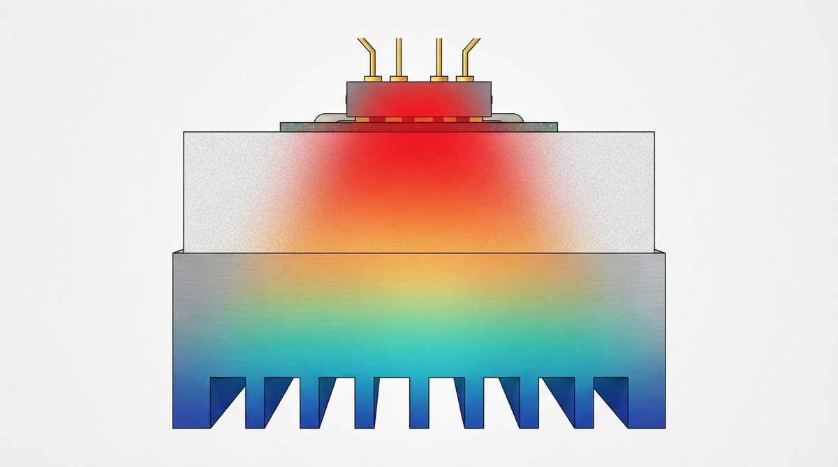
Most ceramic SSR substrates use either 96% alumina or aluminum nitride. The choice depends on the relay’s power dissipation and the thermal budget available in the end system.
| Parameter | 96% Al₂O₃ | AlN | Unit | Condition | Source |
|---|---|---|---|---|---|
| Thermal conductivity | 24–28 | 170–200 | W/mK | 25 °C | Kyocera A-493 / SH-30 datasheets |
| Dielectric strength | ≥ 10 | ≥ 15 | kV/mm | 25 °C, AC | CoorsTek ADS-996 / Maruwa AN datasheets |
| CTE | 7.2–7.4 | 4.5–4.8 | ppm/°C | 25–400 °C | Kyocera datasheets |
| Flexural strength | 350–380 | 300–350 | MPa | ASTM C1161 | CoorsTek / Kyocera |
| Volume resistivity | > 10¹⁴ | > 10¹⁴ | Ω·cm | 25 °C | Kyocera datasheets |
| Relative cost (per cm²) | 1× | 3–5× | — | DBC, 0.635 mm | Industry pricing |
Typical values for commercially available material, for comparison only. Confirm against the datasheet for your specific grade.
For SSRs rated below roughly 10 A at 60 V, 96% alumina often provides enough thermal margin. Above that threshold—or in sealed enclosures with no airflow—a solid state relay AlN PCB becomes the practical choice. The 4.5 ppm/°C CTE of AlN also matches silicon (2.6 ppm/°C) and SiC (4.0 ppm/°C) more closely than alumina does, reducing solder-joint fatigue under thermal cycling. If your SSR uses a bare die rather than a packaged device, that CTE match matters even more. You can explore dielectric properties of ceramic substrates for a deeper comparison of electrical parameters.
Worked Example: Thermal Resistance Through the Substrate
Consider a single-channel SSR dissipating 15 W through a 10 mm × 12 mm die footprint on a 0.635 mm thick substrate. The conduction thermal resistance through the substrate is:
Rth = t / (k × A)
For 96% alumina (k = 26 W/mK):
Rth = 0.000635 / (26 × 0.00012) = 0.204 °C/W → ΔT = 15 × 0.204 ≈ 3.1 °C
For AlN (k = 180 W/mK):
Rth = 0.000635 / (180 × 0.00012) = 0.029 °C/W → ΔT = 15 × 0.029 ≈ 0.44 °C
A 2.6 °C difference at the substrate alone sounds small. But in a real SSR, you also face thermal interface resistance, heatsink resistance, and ambient temperature. Every degree saved at the substrate cascades through the stack. At 44 W dissipation (the 40 A example above), the substrate delta grows to 8.9 °C for alumina versus 1.3 °C for AlN. That 7.6 °C margin can be the difference between meeting and missing a 125 °C junction limit.
Enter your substrate area, thickness, and dissipated power below to estimate junction temperature rise for your own solid state relay AlN PCB design.
Metallization and Assembly Considerations
SSR substrates typically use direct bond copper (DBC) or active metal brazing (AMB) to carry high currents. DBC on AlN requires an oxidation pre-treatment of the AlN surface because copper bonds to an oxide layer, not bare nitride. Reputable substrate suppliers handle this step in-house. AMB skips the oxidation step by using a titanium-containing braze alloy, producing a stronger bond that survives more thermal cycles—important for SSRs that see repeated on/off load surges.
Copper thickness for SSR traces usually falls between 0.2 mm and 0.3 mm (200–300 µm) to handle 20–50 A without excessive I²R heating. Thicker copper increases CTE mismatch stress on the ceramic, so the substrate thickness and copper pattern must be balanced. A symmetrical copper layer on the backside helps counteract bowing. For custom AlN PCB fabrication, specify both copper thickness and back-metallization in your drawing.
Substrate Thickness and Format
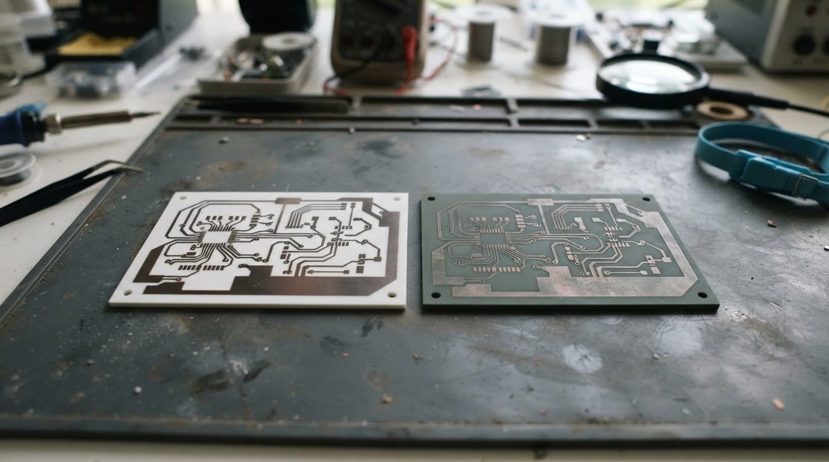
Common AlN substrate thicknesses for SSR use are 0.385 mm, 0.635 mm, and 1.0 mm. Thinner substrates lower thermal resistance but reduce dielectric withstand voltage. A 0.385 mm AlN substrate still provides ≥ 5.8 kV breakdown (15 kV/mm × 0.385 mm), which covers most SSR isolation requirements up to 2.5 kVrms working voltage per IEC 60664-1. For SSRs rated at 4 kVrms isolation, 0.635 mm is the safer choice.
If your design needs a thinner AlN substrate for tighter thermal stacks, AlN thin substrates are available down to 0.25 mm. Confirm the isolation rating against your safety standard before specifying.
When Not to Use a Solid State Relay AlN PCB
AlN is overkill—and overpriced—in several common SSR scenarios:
- Low-current SSRs (≤ 5 A, ≤ 2 W dissipation): 96% alumina handles the heat easily. The substrate cost drops 3–5×. Consider custom 96% alumina fabrication instead.
- SSRs with external heatsinks and forced air: If the system already has a large heatsink and fan, the substrate thermal resistance is a small fraction of total Rth. Alumina is sufficient.
- Cost-sensitive consumer products: For appliance-grade SSRs produced in volumes above 100 k/year, the 3–5× substrate premium rarely pays back in performance.
- Designs that can use packaged devices: If the SSR uses a pre-packaged MOSFET or IGBT module rather than bare die, the package’s internal thermal resistance dominates. Spending on AlN at the board level yields diminishing returns.
Frequently Asked Questions
Can I solder directly to an AlN ceramic PCB?
Yes, but only to the metallized surface—not to bare AlN. DBC and AMB substrates provide a copper layer that accepts standard Sn-Ag-Cu or high-temperature Au-Sn solder. Bare AlN is not solderable without metallization.
Does AlN degrade in humid environments?
Unprotected AlN reacts slowly with moisture, forming aluminum hydroxide on the surface. In SSR applications, the metallization layer and conformal coating or hermetic packaging prevent moisture contact. If the substrate edges are exposed, a passivation coating (e.g., sputtered SiO₂) is recommended.
What is the maximum continuous operating temperature for an AlN SSR substrate?
AlN ceramic itself is stable beyond 1000 °C in inert atmospheres. The practical limit is set by the metallization and solder: DBC copper-to-AlN bonds are rated to roughly 300 °C, and standard SAC305 solder reflows at 217–220 °C. Most solid state relay AlN PCB designs stay below 150 °C at the substrate surface.
How does AlN compare to Si₃N₄ for SSR substrates?
Silicon nitride offers superior fracture toughness (6–7 MPa·m^½ vs. 2.5–3.5 for AlN per CoorsTek data) but lower thermal conductivity (70–90 W/mK). Si₃N₄ is preferred in power modules subject to extreme thermal cycling or mechanical shock. For SSRs where thermal performance is the primary concern, AlN wins.
Is a polished AlN surface needed for SSR die attach?
A polished or lapped surface improves die-attach void rates and thermal interface quality, especially for large die (> 5 mm × 5 mm). For smaller die or solder-based attach, as-fired surfaces with Ra ≤ 0.5 µm are usually adequate. Polished AlN substrates are worth specifying when bond-line thickness control is critical.
Next Step
If your SSR dissipates more than 3–5 W per channel and operates in a thermally constrained enclosure, a solid state relay AlN PCB is the right substrate. Gather your die size, power dissipation, isolation voltage, and copper thickness requirements, then request a ceramic PCB quote from a supplier who fabricates DBC or AMB on AlN in-house.