Ceramic PCB fabrication uses one of five main metallization processes—DPC, DBC, AMB, thick film, or cofired (HTCC/LTCC)—each matched to specific substrate materials and application requirements. Choosing the wrong process for your material or performance target wastes money and lead time, so the first engineering decision is process selection, not material selection.
Key Takeaways
- DPC (direct plated copper) achieves the finest features—line/space down to 50 µm on alumina—making it the default for high-density signal routing on ceramic.
- DBC and AMB bond thick copper (typically 127–500 µm) directly to the substrate for high-current power modules, but minimum trace width is limited to roughly 0.3–0.5 mm.
- HTCC fires at 1 300–1 600 °C and co-sinters tungsten or molybdenum traces with the ceramic; LTCC fires at 850–900 °C and uses silver or gold conductors.
- Substrate material dictates which processes are feasible: AlN works with DPC, DBC, AMB, and thick film, but not LTCC or HTCC in standard production.
- Ceramic substrates are brittle—mechanical handling, panelization, and V-score design all affect yield more than they do on FR-4.
The Five Ceramic PCB Fabrication Processes
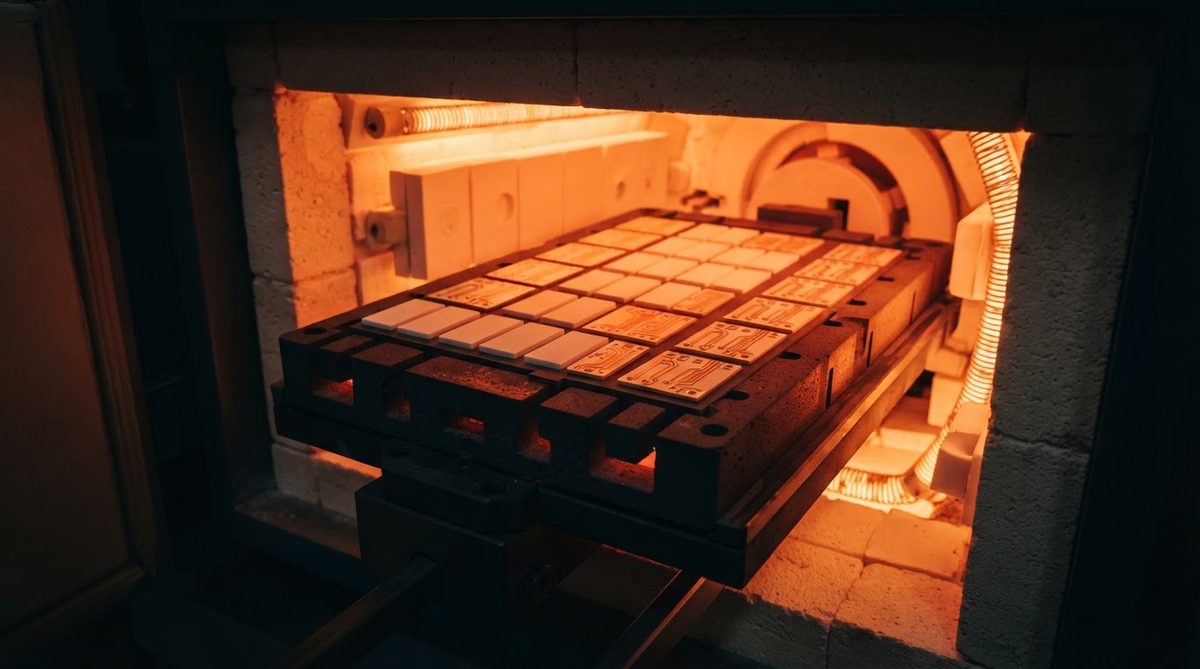
Each fabrication process deposits or bonds metal onto a fired ceramic substrate in a fundamentally different way. The table below summarizes the key differences; the sections that follow explain when each one makes sense.
| Process | Conductor | Min line/space | Cu thickness range | Typical substrates | Best for |
|---|---|---|---|---|---|
| DPC (Direct Plated Copper) | Sputtered seed + electroplated Cu | 50–75 µm | 5–100 µm | Al₂O₃ 96 %, Al₂O₃ 99.6 %, AlN | Fine-pitch signal, RF, LED |
| Thick film | Screen-printed paste (Ag, Au, PdAg) | 100–150 µm | 8–25 µm (fired) | Al₂O₃ 96 %, Al₂O₃ 99.6 %, AlN | Resistor networks, hybrid modules |
| DBC (Direct Bond Copper) | Cu foil oxide-bonded at ~1 065 °C | 300–500 µm | 127–500 µm | Al₂O₃ 96 %, AlN, ZrO₂-toughened Al₂O₃ | IGBT/MOSFET power modules |
| AMB (Active Metal Brazing) | Cu foil brazed via TiAgCu at ~850 °C | 300–500 µm | 127–800 µm | Si₃N₄, AlN, Al₂O₃ | High-reliability power electronics, EV inverters |
| HTCC | W or Mo co-fired at 1 300–1 600 °C | 75–125 µm | 10–20 µm | Al₂O₃ 92–96 % | Hermetic packages, multilayer |
| LTCC | Ag or Au co-fired at 850–900 °C | 75–100 µm | 8–15 µm | Glass-ceramic tape | RF modules, multilayer passives |
Typical values for commercially available material, for comparison only. Confirm against the datasheet for your specific grade.
DPC — Finest Features on Ceramic
DPC starts with a polished, fired substrate. A thin adhesion layer (typically Ti or TiW) and a copper seed layer are sputtered in vacuum, then photoresist is applied and patterned using standard photolithography. Copper is electroplated into the open pattern, the resist is stripped, and the seed layer is etched away. The result is dense, well-adhered copper traces with edge definition comparable to semiconductor packaging.
DPC is the process to specify when your design needs fine pitch (≤ 100 µm line/space), tight impedance control for RF circuits, or high thermal conductivity with thin copper. It pairs well with 96 % alumina custom substrates for cost-sensitive LED and sensor boards, and with aluminum nitride (AlN) custom fabrication when thermal resistance must be minimized.
DBC and AMB — Thick Copper for Power
DBC bonds oxygen-free copper foil to an oxide ceramic (Al₂O₃ or AlN) by forming a thin Cu-O eutectic layer at approximately 1 065 °C. The bond is metallurgical, not adhesive, so thermal resistance through the joint is negligible. DBC substrates carry 127–500 µm copper and handle continuous currents of tens to hundreds of amps.
AMB replaces the oxide bond with a reactive braze alloy containing titanium, which wets non-oxide ceramics. This is the only reliable way to bond thick copper to silicon nitride (Si₃N₄) substrates, whose flexural strength (600–800 MPa per CeramTec data, ASTM C1161) makes them the preferred choice for power modules subjected to deep thermal cycling—EV traction inverters being the most prominent example.
Both DBC and AMB produce coarse features. If your design needs traces narrower than about 300 µm, DPC or thick film is a better fit, potentially on a separate signal layer.
Thick Film — Printed Conductors and Embedded Resistors
Thick-film fabrication screen-prints metal pastes (silver, gold, or palladium-silver) onto the substrate and fires them at 850–950 °C. Resistor and dielectric pastes can be printed in the same sequence, enabling embedded passive networks without discrete components. Line/space resolution is limited to roughly 100–150 µm by the mesh screen, but this is adequate for many hybrid-circuit and sensor applications.
HTCC and LTCC — Cofired Multilayer Ceramic
HTCC and LTCC build multilayer ceramic structures by laminating and co-firing green tape with printed conductor patterns. HTCC uses high-purity alumina tape fired above 1 300 °C; the conductor must survive that temperature, limiting choices to tungsten or molybdenum (resistivity roughly 5–6× higher than copper). LTCC uses a glass-ceramic tape system that fires at 850–900 °C, allowing silver or gold conductors with much lower resistivity.
LTCC is widely used in RF front-end modules and millimeter-wave applications because it supports buried stripline, embedded capacitors, and hermetic cavities. HTCC is favored for hermetic sensor packages and military electronics where alumina’s mechanical properties and hermeticity are mandatory. Neither process is compatible with AlN or Si₃N₄ substrates in standard production.
Material-Process Compatibility Matrix
Not every material works with every process. The matrix below prevents a common specification error: requesting a combination that does not exist in commercial production.
| Substrate | DPC | Thick film | DBC | AMB | HTCC | LTCC |
|---|---|---|---|---|---|---|
| Al₂O₃ 96 % | Yes | Yes | Yes | Yes | Yes | No |
| Al₂O₃ 99.6 % | Yes | Yes | Yes | Yes | No (separate grade) | No |
| AlN | Yes | Yes | Yes | Yes | No | No |
| Si₃N₄ | No (surface too rough) | Limited | No | Yes | No | No |
| Glass-ceramic (LTCC tape) | No | No | No | No | No | Yes |
Si₃N₄ DPC is not standard because as-fired Si₃N₄ surface roughness (Ra > 0.4 µm typical) exceeds what sputtered seed layers tolerate for fine-line patterning. AMB is the standard metallization route for Si₃N₄.
Typical Fabrication Tolerances
Ceramic substrates shrink during sintering (roughly 15–20 % linear for HTCC green tape, near zero for pre-fired DPC/DBC substrates). Tolerances reflect this. The table below covers pre-fired substrate processes; cofired tolerances are wider.
| Parameter | DPC | DBC / AMB | Thick film | Unit | Notes |
|---|---|---|---|---|---|
| Min line width | 50 | 300 | 100 | µm | DPC on polished Al₂O₃ |
| Min space | 50 | 300 | 100 | µm | |
| Cu thickness | 5–100 | 127–800 | 8–25 | µm | AMB upper range |
| Position accuracy | ±25 | ±100 | ±50 | µm | Feature to substrate edge |
| Substrate thickness tolerance | ±25 | ±25 | ±25 | µm | Depends on supplier grade |
| Surface roughness (Ra) | ≤ 0.1 (polished) | 0.3–0.8 | 0.3–0.6 | µm | Post-metallization, copper side |
Typical values; actual limits depend on substrate size, material, and vendor. See ceramic PCB manufacturing capabilities and spec limits for project-specific numbers.
Worked Example: Selecting a Process for a 50 W LED Array
Suppose you need a substrate carrying 24 high-power LEDs dissipating 50 W total, with 0.5 mm pitch between pads. The thermal target is a substrate thermal resistance below 0.3 °C/W. Here is how the process decision flows.
- Pad pitch drives process choice. 0.5 mm pitch means 250 µm pads with 250 µm gaps. DBC’s minimum space of 300 µm fails; DPC at 50 µm line/space passes easily. Thick film at 100 µm passes but with less margin.
- Thermal resistance drives material choice. Using Rth = t / (k × A), with substrate thickness t = 0.38 mm, area A = 30 × 30 mm = 900 mm², and 96 % alumina k = 25 W/mK: Rth = 0.00038 / (25 × 0.0009) = 0.017 °C/W. That is well under 0.3 °C/W, so alumina is sufficient; AlN is not needed.
- Cost check. DPC on 96 % Al₂O₃ is the lowest-cost ceramic fabrication route for this geometry. AlN would add 3–5× material cost with no thermal benefit at this power density.
Result: DPC on 96 % Al₂O₃, 0.38 mm thick, with 20–50 µm electroplated copper and ENIG finish. This is a bread-and-butter ceramic PCB fabrication job, and most suppliers stock the blank substrate.
How Ceramic Fabrication Differs from FR-4 Fabrication
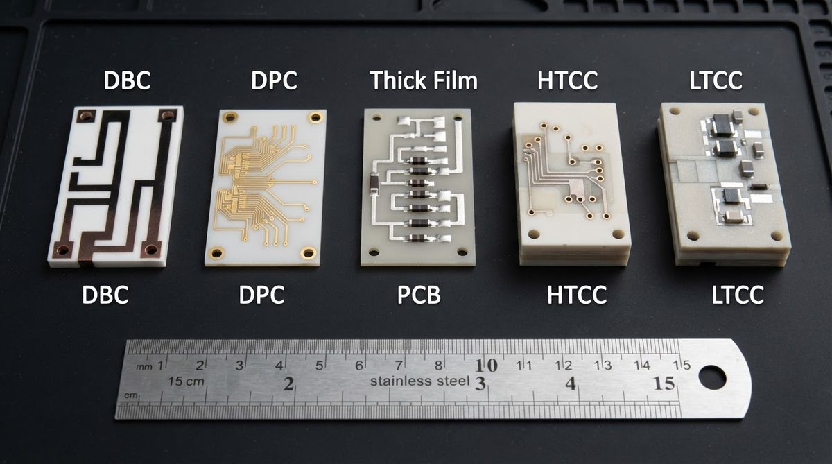
Engineers moving from organic boards to ceramic often underestimate three differences that affect design files and procurement.
No drilling in the traditional sense. Ceramic substrates are too hard for mechanical drilling. Vias and through-holes are formed by laser (DPC, thick film) or punched into green tape before firing (HTCC, LTCC). Minimum via diameter on DPC is typically 100–150 µm; on LTCC, punched vias can go below 100 µm. Plan via placement early—adding vias after substrate firing is expensive or impossible.
For a deeper comparison of each production step, see the full Gerber-to-finished-board production walkthrough.
Panelization and singulation require care. FR-4 panels are routed or V-scored with standard tooling. Ceramic panels are laser-scribed or diamond-saw cut. Scribing must be designed into the substrate layout before firing for cofired processes. Breakout tabs and board edges need larger radii than FR-4 to avoid crack propagation—1 mm minimum fillet radius is a common guideline.
Assembly reflow profiles differ. Ceramic’s high thermal mass and low CTE (6–7 ppm/°C for alumina vs. 14–17 ppm/°C for FR-4) mean soak zones and ramp rates in the reflow profile for ceramic boards must be adjusted to avoid solder joint stress from CTE mismatch with components.
Supply Chain Considerations
Ceramic PCB fabrication involves more specialized vendors than FR-4 production. Blank substrates come from a small number of ceramic manufacturers (CoorsTek, Kyocera, Maruwa, CeramTec). Metallization may be done by a different company than the one supplying the substrate. Understanding who makes what in the ceramic substrate supply chain helps you audit your vendor’s actual capabilities versus what they outsource.
Lead times reflect this complexity. Prototype runs on standard alumina substrates typically ship in 2–3 weeks; AlN or Si₃N₄ substrates with AMB metallization can take 4–8 weeks depending on blank availability. Stock substrate sizes (e.g., 114 × 114 mm, 139 × 190 mm for alumina) ship faster than custom dimensions that require laser cutting from larger panels.
When Not to Use Ceramic Fabrication
Ceramic is the wrong substrate in several common scenarios:
- Low power density, no harsh environment. If your board dissipates under 1 W/cm² and operates between 0 °C and 85 °C, FR-4 or metal-core PCB (MCPCB) will cost 5–20× less and perform adequately.
- Large board area. Standard ceramic substrates max out around 190 × 140 mm for alumina. If your design is 200 × 300 mm, you need tiling or a different technology.
- High mechanical shock. Ceramic substrates fracture under impact. Applications with repeated mechanical shock (handheld consumer devices dropped regularly) are better served by flex or rigid-flex FR-4.
- Dense digital logic with hundreds of vias. Organic HDI boards achieve via densities and layer counts that ceramic cannot match economically. A 12-layer HTCC is possible but rarely cost-justified versus a 12-layer organic HDI.
Frequently Asked Questions
Can I use my existing FR-4 Gerber files for ceramic fabrication?
You can use the same file formats (Gerber RS-274X, ODB++), but the design rules change. Minimum trace, space, via size, and panelization constraints differ by ceramic process. Most fabricators will DFM-check your files and flag incompatibilities before quoting.
What surface finishes are available on ceramic PCBs?
ENIG, ENEPIG, OSP, immersion silver, and bare copper are all used. ENIG is the most common for wire-bondable and solderable pads. Gold thick-film conductors on HTCC/LTCC often need no additional finish. The choice depends on your assembly method and storage conditions.
Is ceramic PCB fabrication RoHS compliant?
Yes. Alumina, AlN, and Si₃N₄ substrates contain no restricted substances under RoHS. DBC uses oxygen-free copper; AMB braze alloys are typically silver-copper-titanium, also compliant. Lead-free solder assembly is standard. Confirm compliance documentation with your specific vendor for each lot.
How do I specify a ceramic board if I have never ordered one before?
Start with five parameters: substrate material, substrate thickness, metallization process, copper thickness, and surface finish. Add your Gerber files and a fabrication drawing with tolerances. A qualified vendor will review the combination for feasibility. For a structured evaluation approach, see the guide on evaluating a ceramic PCB manufacturer.
What is the typical MOQ for ceramic PCB prototypes?
Most ceramic fabricators accept MOQs of 1–5 pieces for prototypes on standard substrate sizes. Custom substrate dimensions or uncommon materials (e.g., 99.6 % alumina, AlN) may require higher minimums—often 10–25 pieces—because the blank substrates themselves have MOQ constraints from the ceramic supplier.
Next Step
If you have a design ready for ceramic fabrication, upload your files for a quick feasibility check and quote. For broader questions about the full ceramic board production sequence, the ceramic PCB manufacturing overview covers each stage from raw substrate to shipped product.