The ceramic PCB supply chain runs through four tiers: raw powder production, substrate sintering, metallization and patterning, and final board fabrication with routing, plating, and test. Most sourcing managers deal only with the last tier, but each upstream stage controls cost, lead time, and quality in ways that matter at the BOM level. Knowing who makes what lets you spec smarter, dual-source earlier, and avoid surprises when a single powder lot delays your entire build.
The Four Tiers of the Ceramic PCB Supply Chain
Unlike FR-4, where a single laminate mill can take you from glass fiber to copper-clad sheet, ceramic PCB production is fragmented across specialists. Each tier adds value and adds weeks.
Tier 1 — Ceramic Powder Production
High-purity alumina (Al₂O₃) powder comes from a handful of global producers: Sumitomo Chemical (Japan), Almatis (Germany/USA), Sasol (South Africa), and Showa Denko (Japan) dominate the 99.5%+ purity grades used in electronics. Aluminum nitride (AlN) powder is even more concentrated; Tokuyama (Japan) and H.C. Starck (now part of Höganäs, Germany) supply most of the high-thermal-conductivity grades. Powder purity, particle size distribution (typically 0.3–2 µm for fine ceramics per ASTM C1274), and oxygen content directly set the final substrate’s thermal conductivity and dielectric strength.
This tier is capital-intensive and slow to expand. A new spray-drying line takes 12–18 months to qualify. When demand spikes—as it did in 2021–2022 with EV power module growth—powder allocation tightens before anything else in the chain.
Tier 2 — Substrate Sintering
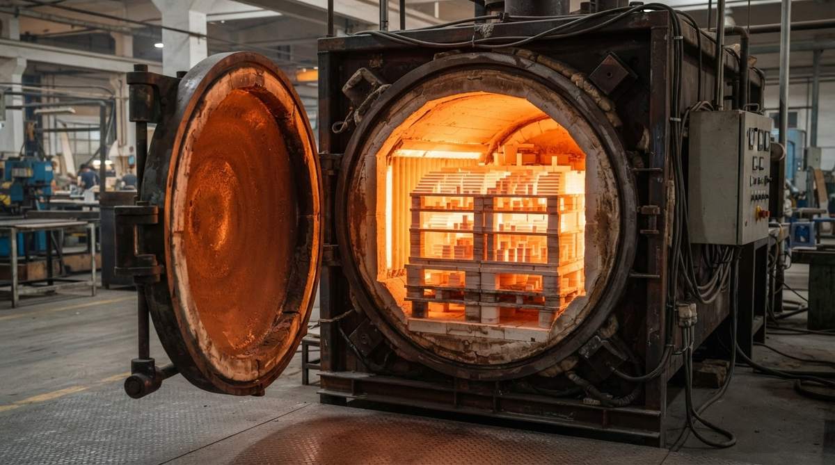
Sintering houses press or tape-cast the powder into green sheets, then fire them at 1,500–1,900 °C (Al₂O₃) or 1,700–1,900 °C (AlN, in nitrogen atmosphere). Major substrate sintering operations include Kyocera, Maruwa, and NTK/NGK (Japan), CoorsTek (USA), and CeramTec (Germany). China-based sintering houses such as Leatec and Sinocera have grown rapidly since 2018, primarily in 96% alumina. Substrate standard sizes and thickness tolerances are set at this stage, and they constrain everything downstream.
Sintering is the longest single lead-time step. Expect 4–8 weeks for standard 96% alumina substrates, 6–12 weeks for 99.6% alumina, and 8–14 weeks for AlN—longer if a non-standard size or thickness is needed.
Tier 3 — Metallization and Patterning
Bare substrates become functional circuits here. The process determines the product category:
- Thick film (screen print + fire): Ag, AgPd, or Au pastes, fired at 850 °C. Widely available; dozens of shops in China, Japan, and Europe.
- Thin film (sputter + etch): Ti/Pt/Au or TiW/Cu stacks, patterned photolithographically to ≤25 µm line/space. Fewer qualified suppliers; capital cost of sputter tools limits capacity.
- DBC (Direct Bond Copper): Oxygen-bonded Cu foil on Al₂O₃ or AlN at ~1,065 °C. Rogers/Curamik (Germany), Toshiba Materials (Japan), and several Chinese DBC lines.
- AMB (Active Metal Brazing): TiAgCu braze bonds Cu to Si₃N₄ or AlN at ~850 °C in vacuum. Heraeus, Kyocera, and Dowa (Japan) are key sources.
- DPC (Direct Plated Copper): Sputter seed + electrolytic Cu plating, achieving fine-pitch traces on alumina or AlN. This is the process used for most high-density ceramic PCBs.
Metallization is where your board fabrication process choice locks in. Switching from DPC to DBC mid-project means re-qualifying the substrate, the trace geometry, and often the solder joint.
Tier 4 — Board Fabrication and Test
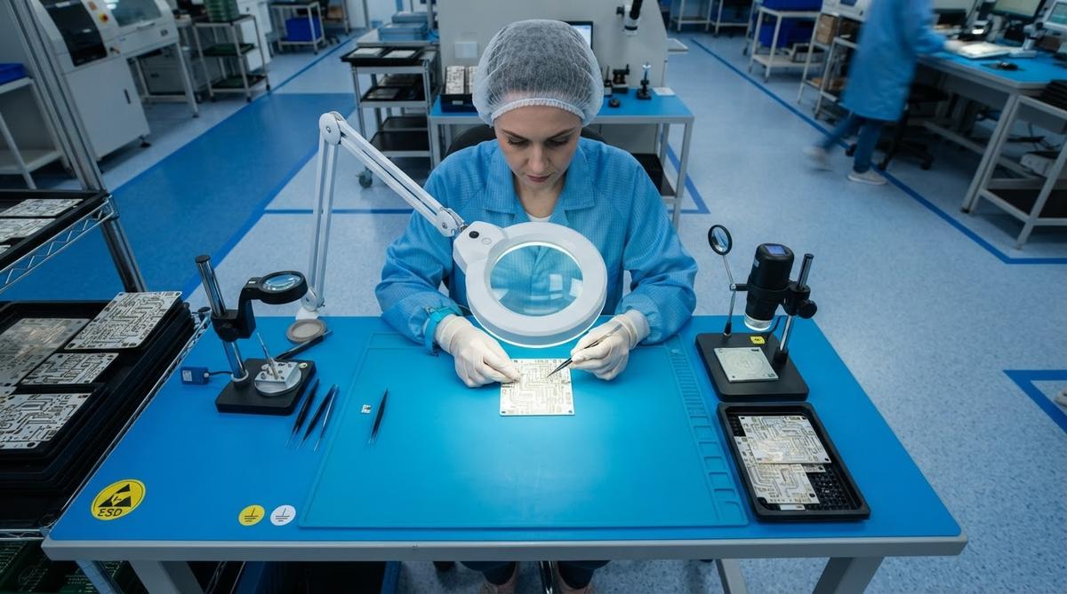
The final tier adds laser or mechanical routing, via drilling, surface finish (ENIG, ENEPIG, OSP, immersion Ag), electrical test, and outgoing inspection. This is the tier most engineers interact with directly. A good Tier 4 shop manages upstream substrate and metallization procurement, buffers inventory on common grades, and owns the test data that ships with your boards.
Who Controls Lead Time—and Where It Gets Stuck
| Supply chain tier | Typical lead time | Bottleneck trigger |
|---|---|---|
| Powder (Tier 1) | 2–6 weeks (if in stock) | Purity upgrade, allocation during EV/5G demand surges |
| Sintering (Tier 2) | 4–14 weeks | Non-standard size, AlN nitrogen furnace scheduling |
| Metallization (Tier 3) | 2–4 weeks | Thin-film sputter queue, AMB vacuum furnace availability |
| Board fab & test (Tier 4) | 1–3 weeks | Custom routing, ENEPIG finish, electrical screening |
Lead times are industry-typical ranges gathered from published supplier data and order experience. Actual times vary by supplier load and specification.
The total for a new ceramic PCB design on AlN with DPC metallization can reach 14–20 weeks from PO to delivery. On 96% alumina with thick film, it can be as short as 4–6 weeks if the substrate sintering house has stock. The single most effective way to compress lead time is to design around standard substrate thicknesses (0.25, 0.38, 0.50, 0.635, 1.0 mm) so Tier 2 can ship from inventory.
Geographic Concentration and Tariff Exposure
Japan dominates Tiers 1 and 2 for high-purity AlN and 99.6% alumina. China leads volume production of 96% alumina substrates and is growing fast in DBC and DPC metallization. Europe (Germany, primarily) holds strong positions in AMB, DBC, and Si₃N₄ substrates through Heraeus, CeramTec, and Rogers/Curamik. The USA has limited sintering capacity (CoorsTek, Accumet) and almost no high-volume DPC or DBC lines.
This geographic split means tariffs and trade policy hit different tiers differently. A U.S. sourcing manager buying finished ceramic PCBs from China faces Section 301 duties, but the underlying AlN powder may originate in Japan and the Cu foil in South Korea. Understanding tariffs and country of origin at the component level prevents surprises on landed cost.
How to Reduce Single-Source Risk
Single-source risk is real in ceramic PCBs. If your design requires AlN substrates with AMB metallization, the global list of qualified suppliers fits on one hand. Here is a practical framework for reducing exposure without over-qualifying:
- Dual-qualify at the substrate level (Tier 2). Approve two sintering sources for the same material grade. Kyocera and Maruwa AlN substrates, for example, are not interchangeable without re-characterization—CTE, thermal conductivity, and camber differ by supplier—but qualifying both up front costs far less than an emergency qualification later.
- Standardize dimensions. Non-standard panel sizes force sole-source sintering. Designing to common substrate formats keeps at least two Tier 2 sources viable.
- Choose a Tier 4 partner that holds substrate buffer stock. A board fabricator with 4–8 weeks of raw substrate inventory absorbs Tier 2 delays without pushing them onto your production schedule.
- Document the full material chain. Ask your Tier 4 supplier for powder origin, sintering source, and metallization process. If they cannot answer, they cannot manage a disruption.
Material-Specific Supply Chain Differences
| Parameter | 96% Al₂O₃ | 99.6% Al₂O₃ | AlN | Si₃N₄ |
|---|---|---|---|---|
| Powder suppliers | Many (Almatis, Sasol, Chinese) | Fewer (Sumitomo, Almatis) | 2–3 (Tokuyama, H.C. Starck) | 2–3 (UBE, Denka) |
| Sintering sources | Dozens globally | ~10 qualified | ~5–8 qualified | ~3–5 qualified |
| Typical substrate cost index | 1× | 2–3× | 4–6× | 6–10× |
| Compatible metallization | Thick film, thin film, DPC, DBC | Thick film, thin film, DPC, DBC | DPC, DBC, AMB, thin film | AMB |
| Substrate lead time (stock sizes) | 2–4 weeks | 4–8 weeks | 6–12 weeks | 8–16 weeks |
Cost index is relative to 96% Al₂O₃ at the same panel size. Actual pricing depends on quantity, size, and surface finish. Lead times assume stock availability at the sintering house.
For choosing the right ceramic substrate, material availability and supply chain depth should factor into the decision alongside thermal and electrical properties—especially for production volumes above 1,000 units per year.
When the Ceramic Supply Chain Is Not Worth the Complexity
If your thermal load stays below 1–2 W/cm² and your operating temperature stays under 130 °C, metal-core PCBs (MCPCBs) on aluminum offer a far simpler supply chain: single-source laminate, standard FR-4 fabrication equipment, 1–2 week lead times. The thermal performance gap only justifies ceramic’s supply chain complexity when you need thermal conductivity above ~8–10 W/mK, hermeticity, or operation above 200 °C.
Similarly, if your volumes exceed 50,000 units/year on a simple single-layer pattern, a thick-film-on-alumina approach sourced entirely from a vertically integrated Chinese supplier may deliver better cost and lead time than a multi-tier DPC chain. Match the supply chain to the application.
Frequently Asked Questions
Can I buy bare ceramic substrates directly from the sintering house?
Yes, if your volumes justify it. Most sintering houses (Kyocera, Maruwa, CoorsTek) sell bare substrates with minimum order quantities of 100–500 pieces for standard sizes. For smaller quantities, a board fabricator that stocks substrates is more practical.
Why is AlN so much more expensive than alumina?
AlN powder costs 8–15× more than alumina powder, and sintering requires nitrogen atmosphere furnaces at higher temperatures (1,750–1,900 °C vs. 1,500–1,650 °C for alumina). The smaller number of qualified sintering sources further limits price competition. Expect finished AlN thin substrates to cost 4–6× more than equivalent alumina parts.
How do I verify the actual material grade in a delivered substrate?
Request a Certificate of Analysis (CoA) from the sintering house that includes XRF composition data, density measurement (per ASTM C373), and thermal conductivity (per ASTM E1461 laser flash). Reputable Tier 4 fabricators pass through the Tier 2 CoA with each shipment.
Does the ceramic PCB supply chain face the same chip-shortage dynamics as semiconductors?
Not identically, but it shares the same demand drivers. EV traction inverters, 5G base stations, and high-power LED modules all consume ceramic substrates. When these markets surge simultaneously, Tier 1 powder and Tier 2 sintering capacity tighten. Lead times stretched 30–50% during 2021–2022. Holding safety stock of substrates is the most common hedge.
What questions should I ask a ceramic PCB supplier about their supply chain?
Ask five things: (1) Where is the substrate sintered, and by whom? (2) What metallization process do you run in-house vs. subcontract? (3) Do you hold substrate buffer stock, and how many weeks’ worth? (4) Can you qualify a second sintering source if I need dual-source? (5) What is your longest recent lead time on this material grade? Vague answers to any of these are a red flag. The ceramic PCB FAQ covers additional procurement questions.