Knowing how to solder ceramic PCB assemblies comes down to managing two risks that barely exist on FR-4: CTE mismatch stress and substrate cracking from thermal shock. You solder to a ceramic PCB the same way you solder to any metallized board — reflow, wave, or iron — but the ramp rate, solder alloy, and fixture design demand more discipline. Get those right, and ceramic boards solder reliably in volume production.
Key Takeaways
- Ceramic substrates (Al₂O₃, AlN, Si₃N₄) have CTEs of 4.5–8.0 ppm/°C, roughly 3–4× lower than FR-4’s 14–16 ppm/°C, so solder joint stress is the primary failure mode.
- Peak reflow temperature for SAC305 on ceramic is the same 240–250 °C as on organic boards, but the ramp rate should stay below 3 °C/s to avoid thermal-shock fracture.
- Active metal brazing (Ti-containing alloys, 800–900 °C) bonds directly to bare ceramic; standard Sn-Ag-Cu solders require a pre-metallized surface (DPC copper, thick-film Ag/Au, or thin-film Ti/Ni/Au).
- Vacuum or forming-gas soldering eliminates voids under high-power die, reaching void rates below 5 % per MIL-STD-883.
Why Learning How to Solder Ceramic PCB Assemblies Matters
The ceramic itself is inert — solder does not wet Al₂O₃ or AlN. Every solderable ceramic board arrives with a metallization layer already bonded to the substrate: DPC copper, DBC copper, thick-film silver or gold, or thin-film Ti/Ni/Au. Your solder joint forms to that metal, not to the ceramic. If the metallization is sound, joint formation is no harder than on a copper-clad FR-4 pad.
The difficulty is what happens after the joint solidifies. As the assembly cools, the ceramic shrinks far less than a copper leadframe or an aluminum heat sink. That differential contraction loads the solder joint in shear. On large-area bonds (power die bigger than 5 × 5 mm), the stress can crack either the solder or the ceramic. Understanding this CTE mismatch is why engineers choose ceramic substrates carefully — the thermal performance is excellent, but the assembly process demands more discipline.
Soldering Methods That Work on Ceramic
Reflow Soldering (Most Common)
Standard SMT reflow with SAC305 paste is the most common way to solder ceramic PCB assemblies in production. Print paste through a stencil, place components, and reflow in a convection or vapor-phase oven. The critical difference from FR-4 reflow is the thermal profile: ceramic’s high thermal conductivity (24–170 W/mK depending on grade) means the board heats more uniformly, but its brittleness demands a controlled ramp. Keep the heating rate at 1.5–3.0 °C/s and the cooling rate below 4 °C/s. Rapid cooling generates tensile stress on the substrate surface and can initiate micro-cracks, especially on alumina thinner than 0.38 mm.
Hand Soldering
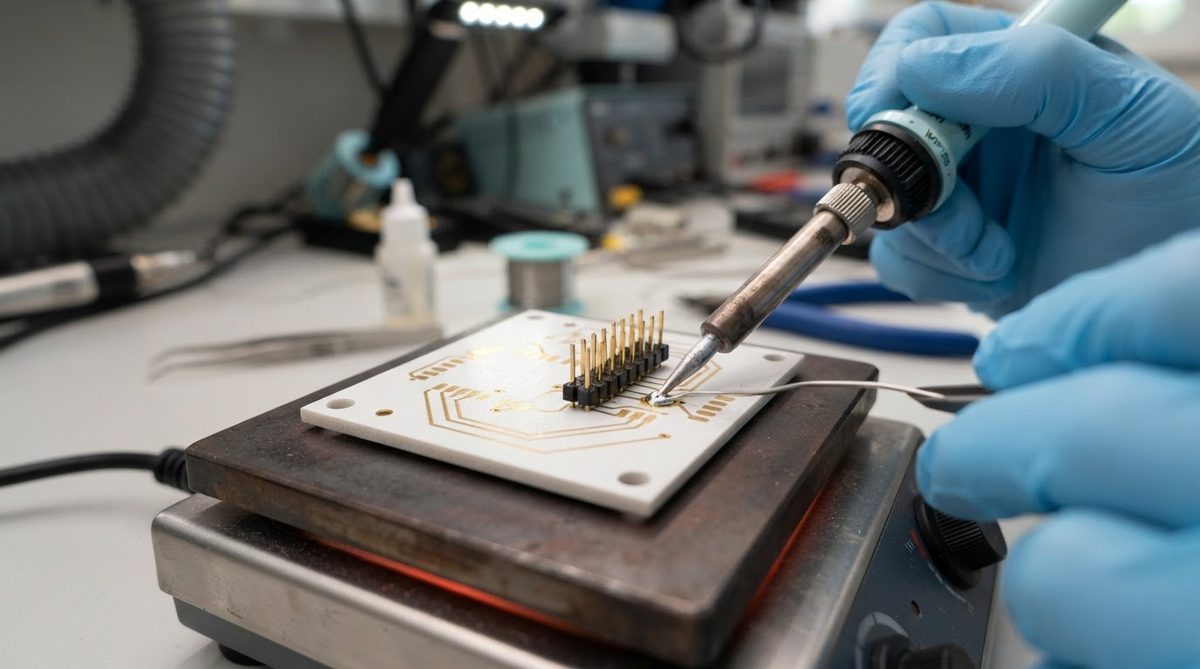
Hand soldering with a temperature-controlled iron (320–370 °C tip) is fine for prototypes and rework. Preheat the board to 100–150 °C on a hot plate first. This reduces the thermal gradient across the substrate and prevents the localized shock that cracks thin alumina. Never press the iron tip hard against the pad — ceramic does not flex. Let the solder flow by heat, not by force.
Vacuum or Forming-Gas Soldering
For power modules where void content under a die must stay below 5 %, vacuum reflow or forming-gas reflow is standard. The reduced atmosphere prevents oxide formation on the solder surface, allowing it to wet fully without flux residue. This method is typical for ceramic PCB substrates used in IGBT modules, SiC half-bridges, and high-brightness LED arrays.
Enter your substrate material, thickness, and target temperature to see how thermal derating affects your soldering window.
Choosing the Right Solder Alloy for a Ceramic PCB
| Alloy | Liquidus (°C) | Typical Use on Ceramic | CTE (ppm/°C) |
|---|---|---|---|
| SAC305 (Sn96.5/Ag3.0/Cu0.5) | 217–220 | General SMT reflow | ~21 |
| Sn63/Pb37 (leaded) | 183 | Mil/aero, legacy assemblies | ~24 |
| Au80/Sn20 | 280 | Hermetic die attach, high-rel | ~16 |
| In50/Pb50 | 209 | Compliant die attach (large die) | ~29 |
| Ag-Cu-Ti (active braze) | 780–900 | Direct bonding to bare ceramic | ~18 |
Values are typical; confirm against your solder supplier’s datasheet for your specific lot.
For a deeper comparison of flux types, paste mesh sizes, and alloy selection for ceramic substrates, see the guide on which solder and paste to use on ceramic.
Step-by-Step: How to Solder Ceramic PCB by Reflow
- Inspect metallization. Check for delamination, discoloration, or oxide. Thick-film silver oxidizes over months in humid storage; if pads look tarnished, clean with isopropyl alcohol or a mild acid dip before printing.
- Print solder paste. Use a laser-cut stainless stencil, 100–125 µm thick for 0402 and larger. Ceramic boards are flat (typical bow < 25 µm over 25 mm), so paste release is usually better than on FR-4.
- Place components. Standard pick-and-place. Support the board from below with a flat vacuum fixture — never clamp the edges of a thin ceramic panel.
- Profile the oven. Preheat zone: ramp at 1.5–2.0 °C/s to 150–180 °C. Soak: 60–90 s. Reflow: peak 240–245 °C for SAC305, time above liquidus 40–70 s. Cooling: ≤ 4 °C/s to 100 °C.
- Inspect. X-ray large ground pads and die-attach areas for voids. AOI for fillet geometry. Ceramic’s flatness makes AOI inspection straightforward.
Worked Example: CTE Mismatch Stress on a 10 × 10 mm Die
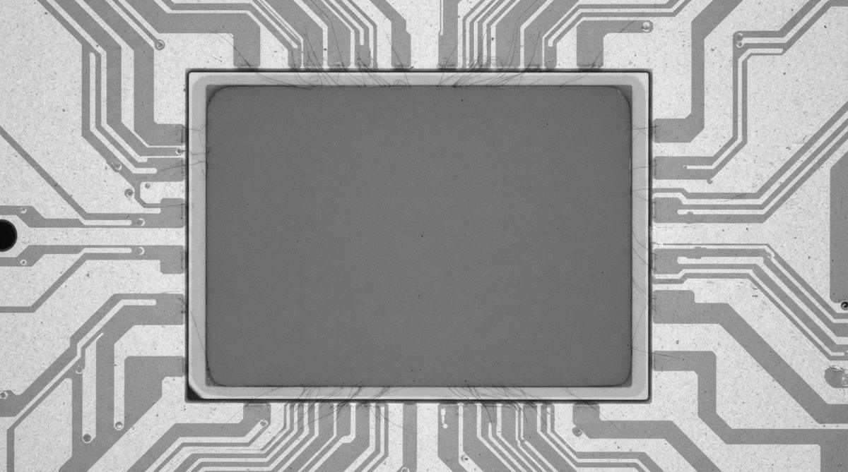
A SiC MOSFET die (CTE ≈ 4.0 ppm/°C) is soldered to a DBC-on-Al₂O₃ substrate (CTE ≈ 7.2 ppm/°C at the copper surface) with SAC305 solder, 100 µm bond line. The assembly cools from 220 °C (solidus) to 25 °C — a ΔT of 195 °C.
Differential strain: (7.2 − 4.0) × 10⁻⁶ × 195 = 6.24 × 10⁻⁴. Over a 10 mm half-diagonal (7.07 mm), the shear displacement at the corner is about 4.4 µm. SAC305 with a 100 µm bond line handles this easily — shear strain is only 0.044, well within the fatigue-safe zone per Engelmaier’s model. If the die were 25 × 25 mm, corner displacement rises to ~11 µm and a more compliant solder (In-Pb) or a thicker bond line becomes necessary.
When Not to Solder a Ceramic PCB
If your assembly involves large mechanical loads, repeated flexing, or drop-shock requirements (consumer handsets, for example), soldering to ceramic is risky. The substrate cannot absorb impact energy the way FR-4 does. A cracked substrate means a scrapped assembly. For those applications, an aluminum-core MCPCB or a flex-rigid FR-4 stackup is a better choice. Ceramic soldering also adds cost: the slower ramp profiles tie up oven time, and rework yield is lower because pads can lift if overheated. If your thermal requirements can be met by a 2 W/mK FR-4 board with thermal vias, the economics rarely justify learning how to solder ceramic PCB assemblies for that project.
Common Mistakes When You Solder Ceramic PCB Assemblies
- Ramp too fast. Exceeding 4 °C/s on a 0.25 mm alumina substrate causes micro-cracks that propagate under thermal cycling. Always profile with a thermocouple on the ceramic surface, not just on a component.
- Wrong flux chemistry. Highly activated (RA) fluxes can corrode thin-film metallization (Ti/Ni/Au stacks under 5 µm total). Use ROL0 or ROL1 flux per IPC J-STD-004B.
- Clamping fixtures. Spring clamps on the board edge concentrate stress. Use vacuum nests or gravity fixtures with compliant (silicone) pads.
- Skipping preheat for hand soldering. A 350 °C iron tip on a room-temperature 0.25 mm AlN coupon creates a >300 °C gradient across millimeters. Preheat to 120–150 °C first.
FAQ
Can I use a standard SMT reflow oven for ceramic PCBs?
Yes. Any convection reflow oven that can run a programmable profile works. The only change is a slower ramp rate (1.5–3 °C/s) and controlled cooling (≤ 4 °C/s). No special atmosphere is needed for standard SMT; vacuum or forming gas is only required for void-critical die attach.
Do I need to bake ceramic boards before soldering?
Ceramic substrates do not absorb moisture the way FR-4 does, so a pre-bake for moisture removal is unnecessary. However, if boards have been stored unsealed for months, a 30-minute bake at 150 °C drives off any adsorbed surface moisture and improves paste wetting. Check ceramic PCB storage and shelf-life guidelines for recommended conditions.
What surface finish is best for soldering ceramic PCBs?
ENIG (electroless nickel / immersion gold) and ENEPIG give the most reliable solder wetting and shelf life. Bare DPC copper works if you solder within days of metallization, but it oxidizes fast. Thick-film silver pads solder well with SAC alloys but require fresh surfaces — silver tarnish inhibits wetting.
Will soldering crack the ceramic?
Soldering itself does not crack ceramic if you control the thermal profile. Cracks come from thermal shock (ramp too fast), mechanical force (pressing an iron tip, clamping fixtures), or CTE-induced stress on very large solder joints. Substrates thicker than 0.38 mm and ramp rates under 3 °C/s virtually eliminate cracking risk in production.
Can I rework a component on a ceramic PCB?
Yes, but with care. Use a focused hot-air rework station, not a chisel tip. Preheat the board to 100–150 °C. Limit rework to two cycles on the same pad — repeated heating can degrade thin-film adhesion layers. Thick-film (Ag, Au) metallizations tolerate more rework cycles than thin-film stacks.