So, what is ceramic PCB? A ceramic PCB is a printed circuit board that uses a ceramic substrate—typically alumina (Al₂O₃), aluminum nitride (AlN), or silicon nitride (Si₃N₄)—in place of the glass-reinforced epoxy (FR-4) found in most electronics. The ceramic base gives the board higher thermal conductivity (24–200 W/mK vs. 0.3 W/mK for FR-4), a wider operating temperature range (up to 800–1 000 °C continuous depending on grade), and better dimensional stability under thermal cycling. Understanding what is ceramic PCB and where it fits matters because these properties make ceramic boards the standard choice for power electronics, RF/microwave modules, LED packages, and sensors exposed to extreme heat or corrosive environments.
Key Takeaways
- Ceramic PCBs operate continuously at 300–1 000 °C depending on the substrate and metallization, versus roughly 130 °C for standard FR-4.
- Alumina 96% (24–28 W/mK at 25 °C) is the most common and least expensive ceramic substrate; AlN (170–200 W/mK) is chosen when thermal resistance must be minimized.
- Ceramic is brittle and costs 5–20× more per unit area than FR-4. It is not the right substrate for every project.
- Common metallization processes include DPC (direct plated copper), DBC (direct bonded copper), AMB (active metal brazing), and thick-film screen printing.
What Is Ceramic PCB Made From? Substrate Materials Compared
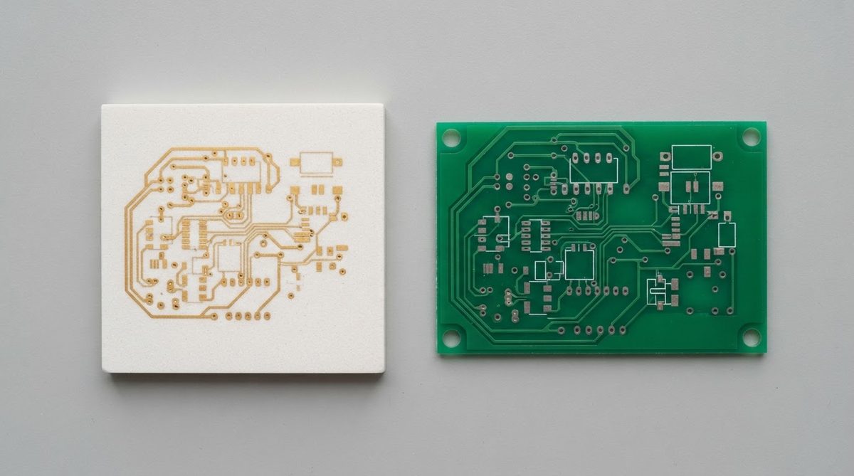
The substrate material determines almost every electrical, thermal, and mechanical property of the finished board. Three ceramics account for the vast majority of production volume.
| Property | Al₂O₃ 96% | AlN | Si₃N₄ | Unit | Condition |
|---|---|---|---|---|---|
| Thermal conductivity | 24–28 | 170–200 | 70–90 | W/mK | 25 °C, per CoorsTek / Kyocera datasheets |
| Dielectric strength | ≥ 10 | ≥ 15 | ≥ 15 | kV/mm | ASTM D149 |
| Flexural strength | 300–380 | 300–400 | 600–900 | MPa | ASTM C1161, 3-pt bend |
| CTE | 7.2–7.4 | 4.5–4.7 | 2.5–3.2 | ppm/°C | 25–400 °C |
| Max continuous use temp | ~1 000 | ~800 (oxidation limit in air) | ~1 000 | °C | Unmetallized substrate |
| Relative cost (Al₂O₃ = 1×) | 1× | 3–5× | 5–8× | — | Approximate, substrate only |
Typical values for commercially available material, for comparison only. Confirm against the datasheet for your specific grade.
Alumina 96% handles most power-LED, sensor, and general high-temperature applications. AlN is the go-to when the thermal path from die to heatsink must be as short and low-resistance as possible—IGBT modules and high-power RF amplifiers are typical examples. Si₃N₄ is chosen where mechanical shock or deep thermal cycling would crack alumina or AlN, such as in EV traction inverters. For a deeper look at reasons engineers choose ceramic substrates, see the dedicated guide.
How Are Ceramic PCBs Made?
Once you know what is ceramic PCB at the material level, the next question is how conductive traces get onto that substrate. The metallization process bonds copper or precious-metal conductors to the ceramic, and each process suits different thickness ranges, feature sizes, and power levels.
- DPC (Direct Plated Copper): Sputtered seed layer followed by electroplating. Achieves fine traces (line/space down to 30–50 µm) on thin copper (1–100 µm). Best for RF, LED, and sensor substrates.
- DBC (Direct Bonded Copper): A copper foil (typically 150–300 µm) is bonded to the ceramic through a thin copper-oxide eutectic layer at ~1 065 °C. Used in power modules carrying tens to hundreds of amps.
- AMB (Active Metal Brazing): A Ti- or Zr-containing braze alloy bonds copper to AlN or Si₃N₄ at ~850 °C. Stronger bond than DBC, preferred for high-reliability automotive and traction inverter modules.
- Thick Film: Screen-printed metal pastes (Ag, Au, Ag/Pd) fired at 850–1 000 °C. Economical for resistor networks, hybrid circuits, and heater elements.
- HTCC / LTCC: Multilayer co-fired ceramic processes. HTCC fires at ~1 600 °C with W or Mo metallization; LTCC fires at ~850 °C with Ag or Au. Both allow buried vias and embedded passives.
If you need to machine or section raw substrates before metallization, the guide on how to cut a ceramic substrate compares five common methods.
Where Are Ceramic PCBs Used?
Power electronics. DBC and AMB substrates carry IGBT and SiC MOSFET die in modules rated from 1.2 kV to 6.5 kV. The ceramic provides electrical isolation and a low-thermal-resistance path to the baseplate.
High-brightness LEDs. Alumina and AlN DPC substrates replace metal-core PCBs when junction temperature must stay below 85 °C at input power densities above 30 W/cm².
RF and microwave. Low-loss tangent (tan δ ≈ 0.0001–0.0003 at 1 MHz for alumina 96%) and tight dimensional tolerance make ceramic substrates standard for filters, couplers, and antenna feeds from L-band through W-band.
Automotive sensors. Exhaust-gas, pressure, and temperature sensors mount directly on alumina thick-film substrates that survive 600 °C+ and thermal shock from −40 °C to 900 °C.
To see how temperature limits interact with substrate choice, the page on ceramic PCB maximum operating temperature provides detailed derating data.
Worked Example: Thermal Resistance Comparison
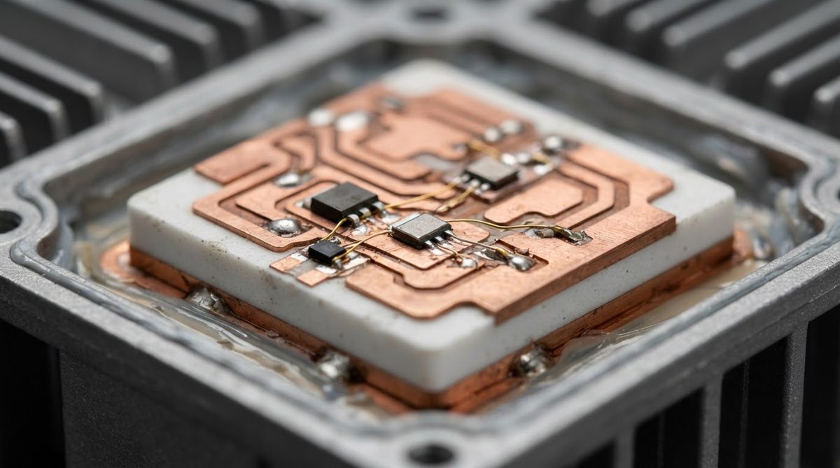
This example shows concretely what is ceramic PCB’s thermal advantage over FR-4. Suppose you have a 10 × 10 mm die dissipating 20 W, mounted on a 1.0 mm-thick substrate. The one-dimensional thermal resistance through the substrate alone (Rth = t / (k × A)) is:
- FR-4: 0.001 m / (0.3 W/mK × 0.0001 m²) = 33.3 °C/W → ΔT = 667 °C. FR-4 cannot handle this.
- Al₂O₃ 96%: 0.001 / (26 × 0.0001) = 0.38 °C/W → ΔT = 7.7 °C.
- AlN: 0.001 / (180 × 0.0001) = 0.056 °C/W → ΔT = 1.1 °C.
The 50× difference between alumina and AlN in ΔT is only 6.6 °C here. At this power density, alumina may be sufficient—saving 3–5× on substrate cost. AlN becomes essential when die area shrinks or power rises further, pushing alumina’s ΔT above design limits.
Enter your own substrate dimensions, material, and power dissipation below to estimate junction temperature rise for your specific design.
When NOT to Use a Ceramic PCB
Ceramic is not a universal upgrade. Choose something else when:
- Cost per board matters more than performance. FR-4 costs roughly $0.01–0.03/cm²; alumina 96% starts around $0.15–0.50/cm² before metallization. If your thermal load fits within FR-4’s limits, ceramic adds cost for no gain.
- You need large panel sizes or many layers. Standard ceramic substrates rarely exceed 150 × 150 mm. Multilayer options (LTCC, HTCC) exist but are expensive above 6–8 layers. FR-4 handles 20+ layers routinely.
- Mechanical shock or drop survival is critical. Ceramic fractures under impact. A metal-core PCB (MCPCB) or flex-rigid FR-4 is tougher in handheld or high-vibration consumer products.
- Rapid iteration on a tight budget. Prototype lead times for ceramic are typically 5–10 business days versus 24–48 hours for quick-turn FR-4.
Frequently Asked Questions
Is a ceramic PCB the same as a metal-core PCB?
No. A metal-core PCB (MCPCB) uses an aluminum or copper base with a thin dielectric layer, typically 75–150 µm of thermally loaded epoxy or polyimide. A ceramic PCB uses the ceramic itself as both dielectric and structural base. Ceramic offers higher dielectric strength and no organic degradation at elevated temperatures.
Can you make a double-sided ceramic PCB?
Yes. Both DPC and DBC processes produce double-sided boards. Electrical connections between sides use filled vias (tungsten in HTCC, copper in DPC) or castellated edge plating. LTCC and HTCC allow true multilayer construction with buried vias.
How thin can a ceramic substrate be?
Alumina substrates are commercially available down to 0.1 mm (100 µm). Thinner substrates are fragile and require careful handling during assembly. See the full discussion on minimum ceramic PCB thickness for design guidance.
Does ceramic PCB need special solder?
Standard SAC305 (Sn96.5/Ag3.0/Cu0.5) solder paste works for most ceramic PCB assemblies, provided the metallization finish is solderable (ENIG, ENEPIG, or Sn plating). High-temperature joints above 300 °C may require Au-Sn or Au-Ge eutectic solders. More detail is in the guide on solder and paste selection for ceramic boards.
Are ceramic PCBs RoHS compliant?
The ceramic substrate itself contains no restricted substances under RoHS. Compliance depends on the metallization and surface finish. Lead-free processes (DPC with ENIG, DBC with Ni/Au) meet RoHS requirements. Thick-film pastes containing PbO-based glass frit may qualify for a high-melting-point solder exemption under RoHS Annex III, but verify with your specific paste supplier.
Next Step
Now that you know what is ceramic PCB and how it compares to conventional substrates, the next move depends on where you are in your project. If you have a board outline, layer count, and target material in mind, upload your files for a quote. For broader questions about ceramic substrates, the ceramic PCB FAQ hub covers sixty common topics in detail.