So, what is a ceramic PCB? It is a circuit board built on a ceramic substrate—most commonly alumina (Al₂O₃), aluminum nitride (AlN), or silicon nitride (Si₃N₄)—rather than on an organic laminate such as FR-4 or polyimide. The ceramic base gives the board higher thermal conductivity (24–200 W/mK vs. 0.3 W/mK for FR-4), a closer coefficient of thermal expansion (CTE) match to silicon and GaN die, and stable dielectric properties from cryogenic temperatures up to 1 000 °C. These properties make the ceramic PCB the default choice for high-power electronics, RF/microwave modules, and sensors that operate in harsh environments.
Key Takeaways
- Alumina 96 % is the most widely used ceramic PCB substrate, offering 24–28 W/mK thermal conductivity at 20 °C and a dielectric constant of ~9.6 at 1 MHz.
- Aluminum nitride reaches 170–200 W/mK, making it the go-to ceramic for direct die-attach of power semiconductors and high-brightness LEDs.
- Common metallization processes include DBC (direct bond copper), DPC (direct plated copper), AMB (active metal brazing), thick film, and thin film—each suited to different power levels, line widths, and cost targets.
- Ceramic substrates are brittle and cost 5–20× more per unit area than FR-4; they are justified only when thermal, frequency, or environmental requirements rule out organic boards.
- Ceramic PCBs are not moisture-sensitive and have an effectively unlimited shelf life when stored properly, unlike organic laminates that absorb water.
What Is a Ceramic PCB Made From? Substrate Materials Compared
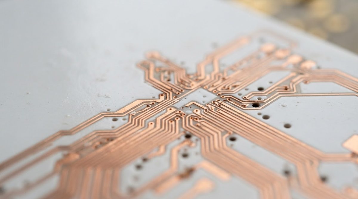
Three ceramics account for the vast majority of production. Each targets a different band of thermal and mechanical requirements.
| Parameter | Al₂O₃ 96 % | Al₂O₃ 99.6 % | AlN | Si₃N₄ |
|---|---|---|---|---|
| Thermal conductivity (W/mK, 20 °C) | 24–28 | 28–33 | 170–200 | 70–90 |
| CTE (ppm/°C, 20–300 °C) | 7.0–7.4 | 7.0–7.2 | 4.4–4.7 | 2.5–3.3 |
| Flexural strength (MPa, ASTM C1161) | 300–380 | 350–400 | 300–400 | 700–900 |
| Dielectric constant (1 MHz) | 9.4–9.8 | 9.8–10.0 | 8.5–9.0 | 8.0–9.0 |
| Max continuous use temp. (°C) | ~1 600 | ~1 700 | ~1 000 | ~1 300 |
| Relative cost (Al₂O₃ 96 % = 1×) | 1× | 1.3–1.5× | 3–5× | 4–7× |
Typical values for commercially available material, for comparison only. Confirm against the datasheet for your specific grade. Sources: CoorsTek ADS-996 datasheet; Kyocera SN-220 datasheet; Maruwa HA-series datasheet.
Alumina (Al₂O₃) is the workhorse. It is inexpensive relative to other ceramics, readily available in thicknesses from 0.25 mm to 2.0 mm, and compatible with every major metallization process. The 96 % grade suits most power and RF applications. The 99.6 % grade is chosen when lower dielectric loss or higher hermeticity matters—common in microwave hybrids and medical implant feedthroughs.
Aluminum nitride (AlN) is selected when the thermal path from die to heatsink must be as short and low-resistance as possible. Its CTE of 4.4–4.7 ppm/°C closely matches silicon (2.6 ppm/°C) and SiC (4.0 ppm/°C), which reduces solder-joint fatigue under thermal cycling. The trade-off is cost and the need for a nitrogen-atmosphere sintering process.
Silicon nitride (Si₃N₄) has the highest fracture toughness of the three. It is used in automotive power modules (IGBT, SiC MOSFET) where the substrate must survive thousands of thermal shock cycles between −40 °C and +175 °C without cracking. Si₃N₄ substrates are metallized almost exclusively by AMB or DBC—not by LTCC or HTCC firing.
How Is a Ceramic PCB Manufactured?
The metallization process determines the minimum feature size, copper thickness, and power-handling capability of the finished board. Here are the five processes you will encounter most often.
DBC – Direct Bond Copper
A copper foil (typically 0.15–0.6 mm) is bonded directly to an alumina or AlN substrate at roughly 1 065 °C in a controlled oxygen atmosphere. The resulting Cu–Cu₂O eutectic wets the ceramic surface. DBC delivers thick copper for high-current paths but limits minimum trace width to about 0.3 mm. It is the standard process for IGBT power modules and EV inverter substrates.
AMB – Active Metal Brazing
A titanium-containing braze alloy (e.g., AgCuTi) bonds copper foil to the ceramic at 800–900 °C under vacuum. AMB produces a stronger bond than DBC and works with Si₃N₄, which DBC cannot reliably bond to. Copper thickness up to 0.8 mm is common. AMB substrates dominate in automotive-grade SiC power modules.
DPC – Direct Plated Copper
Thin-film sputtering deposits a seed layer (Ti/Cu or Cr/Cu) onto the ceramic, followed by photolithographic patterning and electroplating. DPC achieves trace/space down to 30–50 µm, making it the process of choice for RF circuits, LED submounts, and MEMS interposers. Copper thickness is usually 1–100 µm. You can learn more about the patterning step in our guide on etching copper on ceramic substrates.
Thick Film
Screen-printed pastes (silver, gold, palladium-silver, or copper) are fired onto the substrate at 850–1 000 °C. Thick film is the lowest-cost metallization for moderate volumes and is standard for resistor networks, hybrid circuits, and sensor elements. Minimum line width is roughly 100–150 µm.
HTCC and LTCC
High-temperature co-fired ceramic (HTCC) and low-temperature co-fired ceramic (LTCC) build multilayer structures by laminating and co-firing green ceramic tapes with printed conductor layers. HTCC fires at 1 500–1 800 °C using tungsten or molybdenum conductors. LTCC fires at 850–900 °C and can use silver or gold. Both processes are used for complex 3-D RF packages and hermetic sensor housings. Note: HTCC and LTCC are alumina- or glass-ceramic-based processes. They are not used with AlN or Si₃N₄ substrates.
Worked Example: Thermal Resistance Through a Ceramic PCB Substrate
Suppose you are mounting a 10 W laser diode on a 10 mm × 10 mm × 0.635 mm alumina 96 % substrate. The one-dimensional thermal resistance through the ceramic alone is:
Rth = t / (k × A)
Where t = 0.635 × 10⁻³ m, k = 25 W/mK (mid-range for 96 % alumina), and A = 100 × 10⁻⁶ m².
Rth = 0.635 × 10⁻³ / (25 × 100 × 10⁻⁶) = 0.254 °C/W
Temperature rise through the substrate: ΔT = 10 W × 0.254 °C/W = 2.54 °C.
If you swap to AlN (k = 180 W/mK), Rth drops to 0.035 °C/W and ΔT to 0.35 °C—a 7× improvement. Whether that improvement justifies the 3–5× cost premium depends on how tight your thermal budget is. For a 10 W source on this footprint, an alumina ceramic PCB is usually adequate. For a 50 W HEMT on the same footprint, the 12.7 °C rise through alumina may eat most of your margin, and AlN becomes the practical choice.
Enter your own substrate dimensions, material, and power dissipation below to estimate junction temperature rise through the ceramic layer.
Where Are Ceramic PCBs Used?
Ceramic substrates appear wherever one or more of these conditions hold: high junction temperature, high frequency, corrosive atmosphere, or the need for a hermetic package.
- Power electronics: IGBT modules, SiC/GaN half-bridges, EV traction inverters (DBC and AMB on Al₂O₃, AlN, or Si₃N₄).
- LED and UV-C lighting: High-brightness LED submounts, UV-C sterilization arrays where organic substrates degrade under UV exposure.
- RF and microwave: Filters, couplers, antenna feed networks, TR modules up to 77 GHz (thin-film or LTCC on alumina).
- Medical devices: Implantable electronics, endoscope tip assemblies, hearing-aid hybrids—applications that require biocompatibility and hermeticity.
- Aerospace and defence: Radar T/R modules, satellite payload electronics, downhole drilling sensors rated to 200 °C+.
- Automotive sensors: Exhaust-gas sensors (lambda probes), pressure sensors, thick-film heater elements exposed to 300–800 °C exhaust gases.
For a deeper look at the reasons engineers specify ceramic boards, see why use a ceramic PCB.
Ceramic PCB vs. FR-4 and Metal-Core PCB
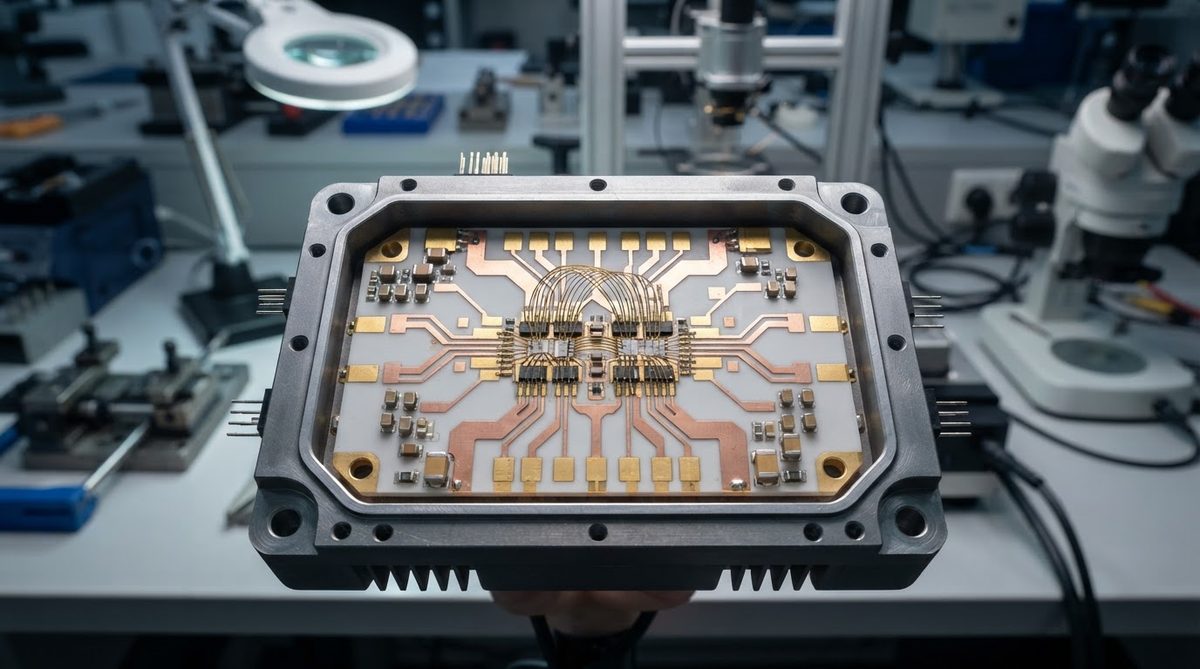
| Parameter | FR-4 | Metal-core (Al base) | Ceramic (Al₂O₃ 96 %) | Ceramic (AlN) |
|---|---|---|---|---|
| Thermal conductivity (W/mK) | 0.25–0.35 | 1–4 (dielectric layer) | 24–28 | 170–200 |
| Max operating temp. (°C) | 130 (Tg-limited) | 130–150 | ~1 000 (metallization-limited) | ~800 (metallization-limited) |
| CTE (ppm/°C) | 14–17 (x-y) | 22–24 (Al) | 7.0–7.4 | 4.4–4.7 |
| Dielectric strength (kV/mm) | 20–30 | 4–8 (dielectric layer) | 10–15 | 14–17 |
| Moisture absorption | 0.1–0.3 % | Negligible (metal) | 0 % | 0 % |
| Relative cost per cm² | 1× | 2–4× | 10–20× | 30–80× |
Typical values for comparison only. FR-4 data per IPC-4101E; MCPCB dielectric layer data per manufacturer specs. Confirm against your specific laminate or substrate grade.
A more detailed comparison between ceramic and metal-core boards is available in our ceramic PCB vs. metal-core guide.
When NOT to Use a Ceramic PCB
Cost-driven consumer electronics. If your board runs below 100 °C, carries moderate current, and operates below 2 GHz, FR-4 or a standard metal-core PCB will work and cost a fraction of a ceramic PCB.
Large board areas. Ceramic substrates are typically limited to panels under 200 mm × 200 mm. If your design exceeds that, you will need to tile multiple substrates or reconsider your architecture.
High mechanical shock. Ceramics are brittle. A board that must survive repeated drop tests (handheld devices, ruggedized tablets) is better served by a flex-rigid or FR-4 construction with conformal coating. Si₃N₄ is tougher than alumina, but it is still far more brittle than epoxy-glass.
Dense digital logic with many layers. Ceramic multilayer (LTCC, HTCC) is possible but expensive for high-layer-count digital boards. If you need 12+ layers of fine-pitch BGA routing, organic HDI is the practical choice.
For a frank discussion of the trade-offs, see ceramic PCB pros and cons.
Frequently Asked Questions
Can you solder components to a ceramic PCB?
Yes. Standard reflow soldering with SAC305 or SnPb paste works on metallized ceramic substrates. The key difference from organic boards is that ceramics have near-zero moisture absorption, so baking before reflow is unnecessary. Use a controlled ramp rate (2–4 °C/s) to avoid thermal shock cracking. More detail is in our guide on choosing solder and paste for ceramic boards.
How thin can a ceramic PCB be?
Alumina substrates are commercially available as thin as 0.1 mm (100 µm). AlN is commonly supplied down to 0.25 mm. Thinner substrates reduce thermal resistance but are more fragile to handle. Production yields drop below 0.25 mm, so expect higher unit costs.
Are ceramic PCBs RoHS compliant?
The ceramic substrate itself contains no restricted substances under RoHS. Compliance depends on the metallization and surface finish. Silver, gold, copper, and nickel finishes are RoHS-compliant. Verify that your solder paste and any thick-film resistor compositions are also compliant.
What is the typical lead time for ceramic PCB prototypes?
Prototype lead times range from 5 to 15 working days depending on the metallization process and substrate material. DPC on alumina is fastest because it uses photolithographic tooling rather than screen-printing screens. LTCC multilayer prototypes take longer—typically 15–25 days—due to the lamination and co-firing steps.
Do ceramic PCBs need conformal coating?
Generally, no. Ceramic substrates do not absorb moisture and are chemically inert, so the substrate itself does not need protection. Conformal coating may still be applied over solder joints and components for salt-fog or condensation resistance, but the motivation is component protection, not substrate protection.
Can a ceramic PCB be reworked?
Yes, but with care. Localised hot-air or infrared rework is standard practice. Avoid rapid thermal gradients above 4 °C/s on alumina or AlN, as this can initiate microcracks. Si₃N₄ tolerates faster ramps thanks to its higher fracture toughness. Always preheat the full substrate to 100–150 °C before localised heating.
Next Step
If your thermal or frequency requirements point toward a ceramic PCB, the next decision is which substrate material and metallization process fit your power density, feature size, and budget. Review the comparison table above, run the thermal resistance calculation for your own die size and dissipation, and request a quote with your Gerber files or mechanical drawing at AluminaPCB.com.