Filled vias in ceramic substrates can achieve void fractions below 2% by area, planarity within ±15 µm, and thermal resistances an order of magnitude lower than open vias of the same diameter. Understanding via filling ceramic capability in full—fill material options, geometry limits, void criteria, and planarity specs—lets you write a via specification that is manufacturable on the first pass. The specific numbers depend on fill material, via geometry, substrate thickness, and firing process. This page sets out the complete capability envelope.
What Is Via Filling on a Ceramic PCB?
Via filling is the process of depositing a conductive or thermally conductive paste into a through-hole or blind via in a ceramic substrate, then co-firing or post-firing it to produce a solid plug. The plug serves one or both of two functions: carrying current between layers, and conducting heat from a die-attach pad to a heatsink plane. On alumina (Al₂O₃) and aluminum nitride (AlN) substrates processed via HTCC or LTCC, vias are typically punched or laser-drilled in the green tape, filled with metal paste, and co-fired in a single cycle. For post-fired substrates metallized by thick-film or thin-film methods, vias are laser-drilled in the sintered ceramic and then filled and re-fired or plated.
Via Filling Ceramic Capability: Fill Materials and Their Properties
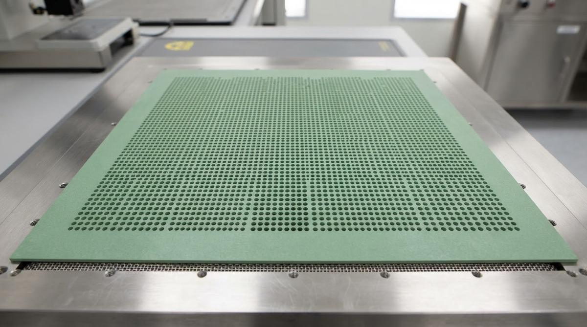
The fill material determines the via’s electrical conductivity, thermal conductivity, CTE match to the substrate, and cost. The table below compares the most common options used in ceramic via filling.
| Fill material | Thermal conductivity (W/mK) | Electrical resistivity (µΩ·cm) | CTE (ppm/K) | Typical use | Source |
|---|---|---|---|---|---|
| Tungsten (W) | 170–180 | 5.3–5.6 | 4.5 | HTCC co-fire with Al₂O₃ | CoorsTek ADS-996 datasheet |
| Molybdenum (Mo) | 138–142 | 5.2–5.7 | 5.1 | HTCC co-fire with Al₂O₃, AlN | Kyocera fine-ceramics catalog |
| Mo-Mn | 100–120 | ~10 | 5.0 | HTCC, hermetic seal packages | CeramTec technical brief |
| Silver (Ag) | 380–420 | 1.6 | 19.7 | LTCC co-fire | DuPont 6141 datasheet |
| Silver-palladium | 200–250 | 3–10 (varies by Pd %) | 15–18 | LTCC co-fire | Ferro LTCC materials guide |
| Copper (Cu) paste | 350–390 | 1.7–2.5 | 17 | Post-fire fill, DPC reflow | Heraeus C8729 datasheet |
Typical values for commercially available material, for comparison only. Confirm against the datasheet for your specific grade.
Tungsten and molybdenum are the default choices for HTCC because their CTE (4.5–5.1 ppm/K) closely matches 96% alumina (6.5–7.0 ppm/K per ASTM E228) and AlN (4.4–4.6 ppm/K). Silver-based fills are standard in LTCC, where the lower co-firing temperature (850–900 °C) allows the use of high-conductivity metals. Copper paste fills are used on post-fired substrates when low resistivity and high thermal conductivity matter more than CTE match, but they require controlled-atmosphere firing or nitrogen reflow to prevent oxidation.
Via Geometry: Diameter, Pitch, and Aspect Ratio Limits
The smallest reliable filled via depends on the drilling method, the substrate thickness, and the fill technique. Green-tape punching for HTCC/LTCC typically achieves smaller diameters than laser drilling sintered ceramic, because the unfired tape is softer and shrinks after firing. These geometry limits define a large part of via filling ceramic capability for any given process.
| Parameter | HTCC (green-tape punch) | LTCC (green-tape punch) | Post-fire laser drill |
|---|---|---|---|
| Min via diameter (finished) | 75–100 µm | 75–100 µm | 100–150 µm |
| Max aspect ratio (depth:diameter) | 3:1 to 5:1 | 2:1 to 4:1 | 2:1 to 3:1 |
| Min via-to-via pitch | 2× diameter typical | 2× diameter typical | 2.5× diameter typical |
| Positional tolerance | ±25–50 µm | ±25–50 µm | ±15–25 µm |
Ranges reflect industry norms across multiple HTCC and LTCC foundries. Request the specific capability sheet for your vendor.
Aspect ratios above 3:1 make complete paste fill difficult and raise the risk of voids. If your substrate is 1.0 mm thick and you need 150 µm vias, the aspect ratio is 6.7:1—well outside the reliable range for most fill processes. In that case, consider stepping down to a thinner substrate (0.38 mm or 0.50 mm) or increasing the via diameter.
Void Fraction and Acceptance Criteria
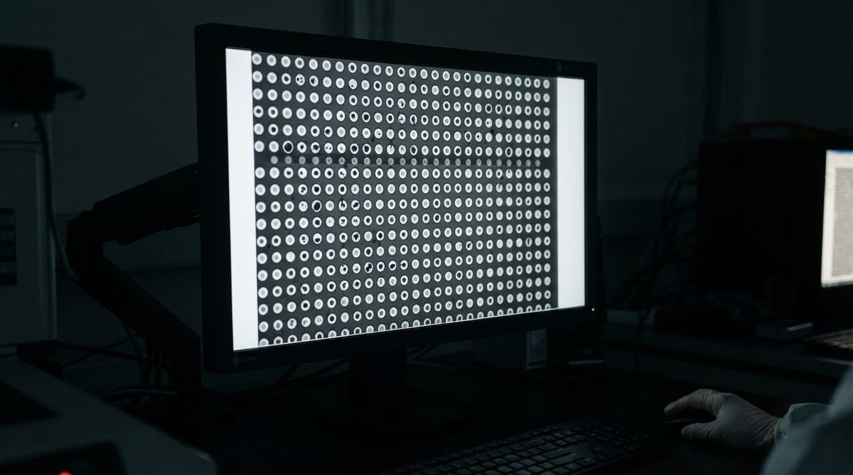
Voids inside a filled via degrade both thermal and electrical performance. The industry-standard inspection method is cross-section analysis or X-ray imaging (per IPC-TM-650, method 2.1.1 for microsectioning). Acceptance criteria vary by application class, and specifying the right class is essential to matching your design to the available via filling ceramic capability at your chosen vendor:
- Commercial / industrial (IPC Class 2 equivalent): void fraction ≤ 5% of via cross-section area.
- High-reliability / military (IPC Class 3 equivalent): void fraction ≤ 2%, no single void larger than 25% of the via diameter.
- Hermetic packages (MIL-STD-883, Method 1014): helium leak rate ≤ 1 × 10⁻⁸ atm·cc/s, which effectively demands near-zero through-going voids.
Worked Example: Thermal Impact of a 5% Void
Consider a tungsten-filled via, 200 µm diameter, 0.635 mm deep, in 96% Al₂O₃. The via’s cross-section area is π × (0.1 mm)² = 0.0314 mm². With zero voids and tungsten at 175 W/mK, the thermal resistance through the via is:
R_th = L / (k × A) = 0.635 mm / (175 W/mK × 0.0314 mm²) = 0.1155 K/mm² → 115.5 K/W
A 5% void reduces the effective conductive area to 0.0298 mm², raising R_th to about 121.6 K/W—a 5.3% increase. For a single via carrying 0.5 W, that adds roughly 3 °C. Across an array of 25 thermal vias in parallel, the per-via power is lower but the aggregate effect still matters in designs targeting junction temperatures near the limit.
Enter your via diameter, substrate thickness, fill material, and estimated void fraction to see the resulting thermal resistance per via and per array.
Planarity and Surface Finish After Filling
After firing, the via fill may be recessed (underfill) or proud (overfill) relative to the substrate surface. For die attach and wirebonding, planarity matters. Typical capabilities:
- Co-fired HTCC/LTCC: ±10–25 µm from the substrate surface, as-fired.
- Post-fire filled vias, lapped: ±5–10 µm planarity after lapping.
- Plated-over filled vias: the copper plating step can planarize to ±5 µm with a flash-etch or chemical-mechanical polish.
If your assembly process uses solder paste stencil printing, via dimple or bump height must stay within the stencil thickness tolerance. A 100 µm stencil with ±25 µm via planarity can produce solder volume variations exceeding 20%.
Design Rules for Reliable Via Fill
These rules reduce fill defects and improve first-pass yield. They reflect the practical via filling ceramic capability across HTCC, LTCC, and post-fire processes:
- Keep aspect ratio ≤ 3:1. If depth exceeds 3× diameter, use stacked vias across multilayer ceramic builds instead of a single deep via.
- Use a capture pad ≥ 1.5× via diameter on both sides to allow paste overflow and prevent delamination.
- Maintain ≥ 2× pitch. Closer spacing causes paste bridging and makes X-ray inspection unreliable.
- Match fill CTE to substrate. A CTE mismatch above 4 ppm/K between fill and ceramic risks cracking during thermal cycling (per IEC 60068-2-14, –55 °C to +125 °C, 500 cycles).
- Specify void criteria on the drawing. If you need Class 3, call it out. Vendors will not inspect to a tighter standard than you request.
When Not to Use Filled Vias
Filled vias add cost and process steps. Skip them when:
- Thermal load is modest. If the total dissipation is under 1 W/cm² and the substrate itself conducts enough heat laterally, open plated-through vias or simple metallized holes may suffice.
- Single-layer design. No interlayer connection is needed, and thermal vias can be replaced by a direct backside metallization and solder attach.
- Cost is the primary driver. Filled vias on post-fired substrates require an extra drill, fill, and fire cycle. For high-volume consumer products, an aluminum-core MCPCB with standard PTH vias is often cheaper and adequate.
- Very thick substrates (> 1.0 mm). Aspect ratio limits make reliable fill impractical. Consider a thinner substrate or a via-in-pad alternative with partial fill instead.
Frequently Asked Questions
Can filled vias in ceramic handle reflow soldering temperatures?
Yes. Co-fired tungsten and molybdenum fills are sintered at 1,500–1,600 °C, so a 260 °C lead-free reflow profile is well within their range. Silver-filled LTCC vias, fired at 850–900 °C, are equally stable at reflow. The substrate itself is the limiting factor, and alumina and AlN tolerate reflow without issue.
How do I inspect filled vias for voids?
X-ray imaging is the standard non-destructive method. It reveals internal voids and their approximate size. For qualification lots, destructive cross-sectioning per IPC-TM-650 method 2.1.1 gives exact void fraction and fill adhesion data. Specify the inspection method and acceptance criteria in your purchase order.
What happens if the via fill cracks during thermal cycling?
A cracked fill increases electrical resistance and thermal resistance. In hermetic packages, it breaks the seal. Cracks most often originate from CTE mismatch or excessive void fraction. Choosing a fill material within 2 ppm/K of the substrate CTE and holding voids below 2% eliminates most cracking failures through 1,000 cycles of –55 °C to +150 °C.
Is copper fill compatible with alumina substrates?
Copper paste can fill vias in post-fired alumina, but the CTE gap is large (17 ppm/K for Cu vs. 6.5–7.0 ppm/K for 96% Al₂O₃). This limits reliability under wide thermal cycling. Copper fill works well for moderate thermal excursions (0 °C to +85 °C) and where the via is short (substrate ≤ 0.38 mm), keeping shear stress low.
Do filled vias affect impedance control on RF ceramic boards?
Filled vias change the effective dielectric environment around signal traces routed near them. For controlled-impedance lines, keep signal traces at least 3× via diameter away from any filled via. Ground vias filled with the same metal as the trace metallization cause fewer discontinuities than mixed-metal fills. Reviewing the full via filling ceramic capability of your vendor’s RF process is important before committing to a stackup.