Thick film ceramic PCBs typically cost $2–$8 per piece in production volumes of 1,000+, assuming a single-substrate design on 96% alumina with one or two conductor layers. Understanding thick film ceramic cost upfront lets you make smarter trade-offs before committing to a layout. Prototypes in quantities under 50 can run $15–$50 each because screen and tooling charges are amortized over fewer units. The exact price depends on six factors, each of which you can influence at the design stage.
Six Drivers Behind Thick Film Ceramic Cost
Every thick film quote is shaped by the same set of variables. Understanding them lets you trade off performance against budget before you lock in a design. For a broader view of how ceramic PCB costs compare across technologies, the pillar page covers DPC, DBC, HTCC, and LTCC alongside thick film.
| Cost driver | Low-cost choice | Higher-cost choice | Typical impact |
|---|---|---|---|
| Substrate material | 96% Al₂O₃ | AlN or 99.6% Al₂O₃ | 2–5× base price |
| Substrate size | ≤ 25 × 25 mm | > 50 × 50 mm | Larger panels yield fewer parts |
| Number of print-fire layers | 1 conductor + 1 resistor | 3+ conductor layers | Each layer adds 15–25% |
| Paste chemistry | Silver (Ag) | Gold (Au) or PdAg | Au paste can add $0.50–$2.00/pc |
| Line/space resolution | ≥ 200 µm / 200 µm | < 125 µm / 125 µm | Tighter rules need finer screens, slower print |
| Post-fire processing | None | Laser trim, plating, ENIG | Laser trim adds 10–20% |
Ranges are order-of-magnitude guides. Request a project-specific quote for binding numbers.
Substrate Material: The Biggest Single Line Item in Thick Film Ceramic Cost
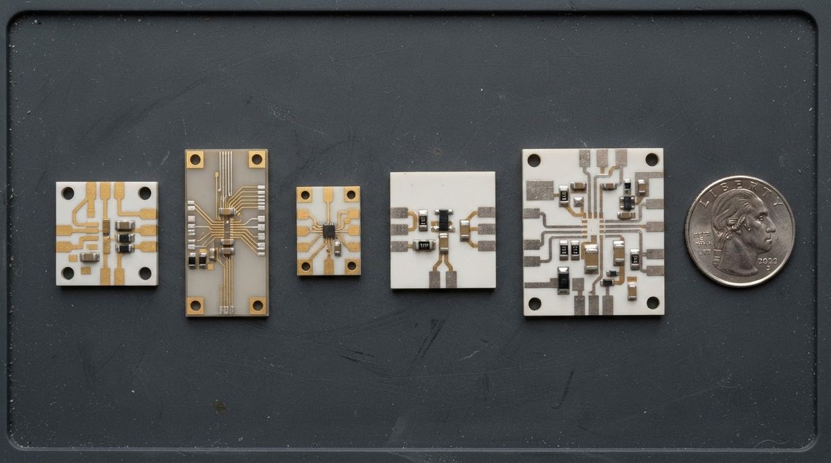
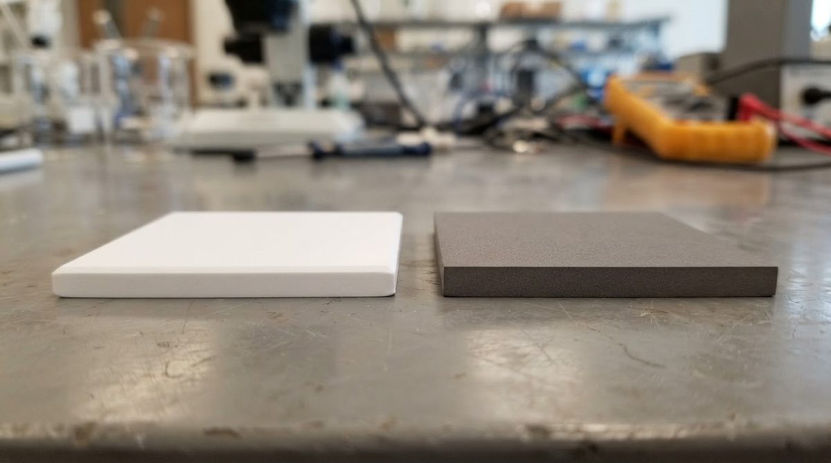
The blank ceramic substrate often accounts for 30–50% of the finished piece price. A standard 96% alumina thick film substrate is the workhorse grade: widely available, screen-printable with standard pastes, and the cheapest option per square centimeter. Moving to aluminum nitride (AlN) thick film substrates multiplies the substrate cost by roughly 3–5× because of higher raw-material and sintering costs, though the thermal conductivity jump from 24–28 W/mK to 170–200 W/mK may be worth it for high-power designs.
99.6% alumina sits in between: about 1.5–2× the price of 96% alumina, with better surface finish and marginally higher thermal conductivity (28–32 W/mK). Choose it when you need tighter line resolution or improved hermeticity, not just thermal performance.
Paste Chemistry and Precious-Metal Pricing
Thick film conductors are screen-printed from pastes containing metal particles in a glass frit binder. The metal choice directly affects thick film ceramic cost:
- Silver (Ag): Lowest cost, best conductivity (~1.6 µΩ·cm sheet resistivity for fired films). Susceptible to electromigration at high humidity and DC bias. Good default for most industrial and LED applications.
- Gold (Au): Excellent wire-bondability and corrosion resistance. Paste price tracks the London gold fix; at $2,300/oz Au, expect $0.50–$2.00 added per piece depending on coverage area.
- Palladium-silver (PdAg): Solder-leach resistant, mid-range cost. Common in automotive sensor substrates where solder joint reliability matters.
If your design uses silver metallized ceramic conductors, verify that your operating environment does not promote silver migration. The paste is cheap; field failures are not.
Worked Example: Pricing a Typical Sensor Substrate
Assume a 25 × 25 mm, 0.635 mm thick, 96% Al₂O₃ substrate with one Ag conductor layer, one RuO₂ resistor layer, and a glass overcoat. No laser trim, no plating. This example illustrates how each process step contributes to the total thick film ceramic cost.
| Item | Est. unit cost (1,000 pcs) | Notes |
|---|---|---|
| Blank substrate | $0.80 | Panelised, scribed |
| Screen tooling (amortised) | $0.30 | 3 screens at ~$100 each |
| Ag conductor print + fire | $0.60 | One pass, peak 850 °C |
| Resistor print + fire | $0.50 | RuO₂-based paste |
| Glass overcoat print + fire | $0.30 | Protection layer |
| Inspection and packing | $0.20 | Visual + continuity |
| Total | ~$2.70/pc |
Estimates based on typical contract-manufacturing pricing in Asia, mid-2025. Your quote will vary with paste coverage area, yield, and supplier.
If you switched the substrate to AlN and the conductor to Au, the same footprint would land closer to $12–$15 per piece—roughly 5× the alumina/Ag version.
Enter your substrate dimensions, layer count, and paste metal below to generate a rough cost estimate for your own design.
How to Reduce Thick Film Ceramic Cost Without Cutting Corners
Panelise aggressively. Fitting more units per panel spreads the substrate and print-cycle cost. Follow the thick film layout guidelines to maximise panel utilisation while keeping snap-off tabs clean.
Minimise print-fire cycles. Every additional layer means another screen, another print pass, and another trip through a belt furnace at 850 °C. Combining conductor and resistor functions on the same layer is not possible, but eliminating a redundant overcoat or consolidating two conductor layers into one can save 15–25% per eliminated cycle.
Relax line/space where you can. A 200 µm line/space design prints on a standard 325-mesh screen. Dropping to 125 µm requires a finer mesh, slower print speed, and tighter process control. Keep fine features only where the circuit demands them.
Choose Ag unless the application forbids it. Gold and PdAg pastes exist for good reasons, but silver handles most thermal, LED, and sensor applications at a fraction of the paste cost.
Thick Film vs. Thin Film: When the Price Gap Narrows
Thick film is almost always cheaper than thin film for the same substrate size and material. Thin film uses sputtered or evaporated metals and photolithographic patterning, which adds capital-intensive vacuum steps. However, the gap narrows when you need features below 50 µm or resistor tolerances tighter than ±1%. At that point, thick film requires laser trimming on every unit, and the per-piece thick film ceramic cost can approach or exceed thin-film ceramic pricing. If your design sits in that grey zone, get quotes for both processes.
When Thick Film Is Not the Right Choice
Thick film is a poor fit when your design needs sub-25 µm traces, multi-layer buried vias (consider HTCC or LTCC), or very high current capacity above 10 A per trace (consider DBC or thick copper). It is also unnecessary when standard FR-4 meets your thermal and frequency requirements—FR-4 at $0.10–$0.30 per piece will always undercut ceramic on price alone. Use thick film ceramic when you need the combination of high operating temperature, low CTE mismatch to semiconductors, and moderate conductor resolution that organic boards cannot provide.
Frequently Asked Questions
How much does thick film tooling cost?
A single thick film screen typically costs $80–$150. A three-layer design (conductor, resistor, overcoat) therefore requires $240–$450 in screen tooling. Screens last 5,000–20,000 prints before replacement, so the amortised cost per piece drops below $0.10 at volumes above 2,000.
Does substrate thickness affect price?
Yes. Standard thicknesses (0.25 mm, 0.38 mm, 0.635 mm, 1.0 mm) are stocked by most suppliers and cost the least. Non-standard thicknesses require custom lapping or special sintering runs, adding 20–40% to the substrate cost.
Are there minimum order quantities for thick film ceramic?
Most ceramic PCB manufacturers accept prototype orders as low as 5–25 pieces, but the per-piece price will be high because tooling and setup costs dominate. Cost-effective production generally starts around 500–1,000 pieces.
Can I get a budgetary price before finalising my design?
Yes. Provide the substrate material, approximate dimensions, number of conductor and resistor layers, paste metal, and expected annual volume. That is enough for a ±20% budget estimate from most suppliers.
Does laser trimming of resistors add significant cost?
Laser trimming adds roughly 10–20% to the finished piece price. It is standard practice when resistor tolerance must be tighter than ±10%, which is the typical as-fired tolerance for thick film resistors. If your circuit can tolerate ±10–20%, skip the trim and save the cost.