Thick Film Definition
The thick film definition in ceramic PCB manufacturing is straightforward: thick film is an additive metallization process in which conductive, resistive, or dielectric pastes are screen-printed onto a ceramic substrate and fired at 850–1000 °C. The resulting layers are typically 10–50 µm (0.4–2.0 mil) thick. This distinguishes the process from thin-film metallization, which deposits material by sputtering or evaporation at sub-micron thicknesses.
Thick film is the most widely used metallization method for ceramic PCBs, hybrid circuits, and chip resistors. It works on alumina (Al₂O₃), aluminum nitride (AlN), and other oxide or nitride ceramics. Understanding the thick film definition helps engineers decide whether screen-printed conductors suit their design or whether a finer-pitch process is needed.
How the Thick Film Process Works
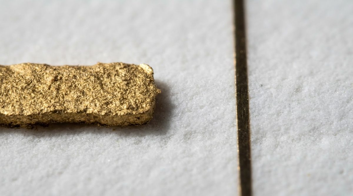
- Paste preparation. A metal or metal-oxide powder (silver, gold, palladium-silver, or copper) is mixed with a glass frit binder and an organic vehicle to form a printable ink.
- Screen printing. The paste is forced through a patterned stainless-steel mesh onto the ceramic substrate. Each print defines one functional layer: conductor, resistor, or dielectric.
- Drying. The wet print is dried at 100–150 °C to remove solvents.
- Firing. The substrate passes through a belt furnace at 850–1000 °C (peak, typically 850–900 °C for silver-based pastes). The glass frit melts, bonds the metal particles to the ceramic, and the organic binder burns away.
- Repeat. Multi-layer circuits go through additional print-dry-fire cycles, one layer at a time.
For detailed conductor widths, spacings, and layer counts, see the thick film ceramic design rules page.
Typical Materials and Properties
| Parameter | Typical Range | Notes |
|---|---|---|
| Layer thickness | 10–50 µm | Per print; multiple prints can build thicker layers |
| Conductor materials | Ag, Au, Pd-Ag, Cu | Cu requires nitrogen-atmosphere firing |
| Min line / space | 100–150 µm (4–6 mil) | Depends on mesh count and paste rheology |
| Sheet resistance (conductor) | 2–20 mΩ/□ | Ag-based pastes at the low end |
| Firing temperature | 850–1000 °C | Per paste manufacturer datasheet |
Typical values for commercially available materials, for comparison only. Confirm against the datasheet for your specific paste and substrate grade.
Thick Film vs Thin Film — How the Definitions Differ
| Attribute | Thick Film | Thin Film |
|---|---|---|
| Deposition method | Screen printing | Sputtering / evaporation |
| Layer thickness | 10–50 µm | 0.05–2 µm |
| Min line / space | 100–150 µm | 10–25 µm |
| Tooling cost | Low (screens) | Higher (photomasks, vacuum equipment) |
| Best for | Power circuits, heaters, general interconnect | RF, precision resistors, fine-pitch |
By the standard thick film definition, any screen-printed and fired layer above roughly 10 µm qualifies. Thick film is the better choice when line widths above 100 µm are acceptable and cost matters more than feature density. Thin film wins for RF impedance control and features below 50 µm.
Use the tool below to compare key properties of thick film and thin film side by side for your specific substrate and application.
Common Substrates for Thick Film
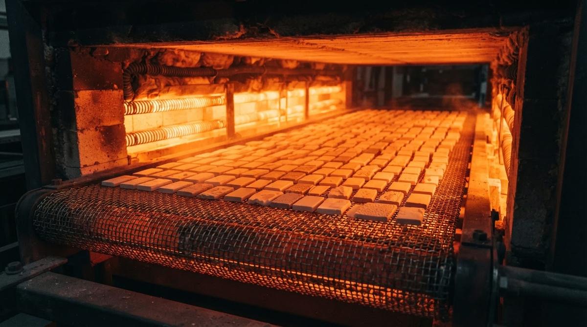
The most common substrate is 96% alumina. Higher-purity 99.6% Al₂O₃ thick film ceramic is used where lower dielectric loss or higher thermal conductivity is needed. AlN substrates accept thick film pastes formulated for nitrogen firing, serving high-power thermal applications.
When Thick Film Is Not the Right Choice
If your design requires trace widths below 50 µm, or resistor tolerances tighter than ±1% without laser trimming, thin-film metallization is a better fit. For very high current loads demanding copper layers above 300 µm, direct-bonded copper (DBC) or active metal brazing (AMB) processes are more appropriate than screen-printed conductors. In those cases, the thick film definition simply does not cover the performance you need.
Frequently Asked Questions
What does the thick film definition mean in practice?
In practice, the thick film definition refers to any ceramic metallization layer deposited by screen printing and high-temperature firing, resulting in a film thickness of 10–50 µm. It is the default process for most hybrid circuits and ceramic PCB interconnects where feature sizes above 100 µm are acceptable.
Can thick film conductors carry high current?
Yes, but within limits. A single-print silver conductor at 25 µm thickness can handle moderate current densities suitable for most signal and low-power circuits. For currents above a few amps per trace, multiple print passes or wider conductors are needed. Beyond roughly 10 A, DBC or AMB copper layers are a better option.
Is thick film compatible with wire bonding?
Thick film gold and palladium-silver pads are routinely wire-bonded in hybrid assemblies. Surface roughness from screen printing is higher than thin-film pads, so bond pull strength should be validated during qualification. For guidance, refer to the wire bonding glossary entry.
How does thick film firing temperature affect substrate choice?
Standard silver-based pastes fire at 850–900 °C, which is well within the capability of alumina and AlN substrates. Copper pastes require a nitrogen atmosphere but similar peak temperatures. LTCC substrates co-fire with thick film pastes at around 850 °C, while HTCC alumina fires at much higher temperatures (1400–1600 °C) before thick film layers are added in a post-fire step.
Related Terms
See the full ceramic PCB glossary for definitions of DBC, LTCC, HTCC, and other metallization methods.