Ceramic firing sintering — the thermal process that converts a compacted ceramic powder body (the “green” body) into a dense, hard substrate — dictates nearly every property a ceramic PCB designer cares about. Final density, grain size, dimensional tolerance, thermal conductivity, and metallization compatibility all trace back to what happened in the kiln. HTCC alumina fires at 1 500–1 700 °C and requires refractory metals; LTCC glass-ceramic fires at 850–950 °C and accepts silver or gold co-firing. Understanding ceramic firing sintering is essential whether you specify co-fired circuits or buy pre-sintered blanks for DPC or thin-film processing.
Key Takeaways
- HTCC Al₂O₃ 96 % sinters at 1 500–1 600 °C for 2–6 hours, reaching ≥ 95 % theoretical density and 24–28 W/mK thermal conductivity (per CoorsTek ADS-996 datasheet).
- LTCC tapes sinter at 850–950 °C, enabling co-firing with Ag or Au conductors that would melt at HTCC temperatures.
- Lateral shrinkage during ceramic firing sintering is typically 12–17 % for HTCC and 12–16 % for LTCC, and must be compensated in artwork scaling.
- AlN requires sintering at 1 750–1 900 °C in a nitrogen atmosphere with yttria sintering aids to reach 170–200 W/mK.
- Post-sintered (pre-fired) substrates used in DPC and thin-film processes skip co-firing entirely — metallization happens after the substrate is already dense.
What Happens During Ceramic Firing Sintering
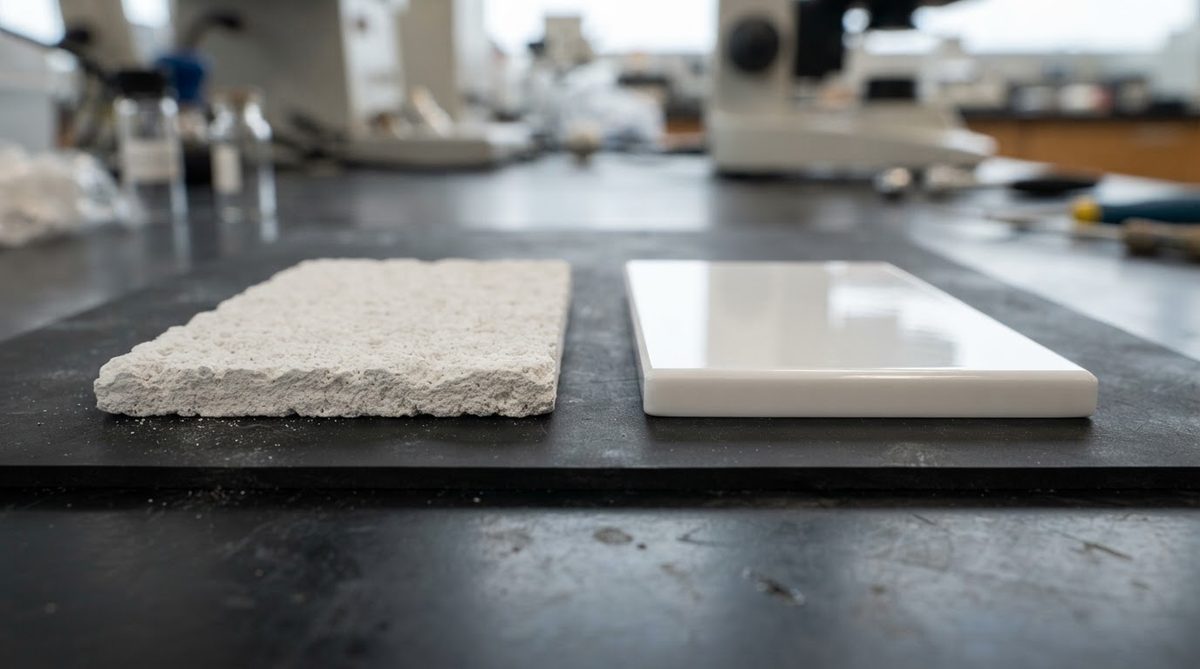
Ceramic firing sintering is a solid-state diffusion process. Ceramic powder particles bond at their contact points when heated to 50–80 % of the material’s absolute melting temperature. Pores shrink, grain boundaries migrate, and the body densifies. No melting of the primary ceramic phase occurs. The driving force is a reduction in total surface energy as small particles merge into larger grains.
A typical firing cycle has three stages: binder burnout (200–600 °C), ramp to peak temperature, and a soak at peak temperature followed by controlled cooling. The binder burnout phase is critical. Organic binders in the green tape or pressed body must decompose completely before the ceramic begins to densify; trapped carbon causes black-coring defects and reduces dielectric strength. Ramp rates during burnout are usually held to 1–3 °C/min for thick parts.
Final density is the primary quality metric. For 96 % alumina, the target is ≥ 3.72 g/cm³ (≥ 95 % of theoretical density of 3.92 g/cm³). Under-sintered substrates have lower thermal conductivity, reduced flexural strength, and higher porosity that traps plating chemicals in later processing steps.
HTCC Firing: Temperatures, Atmospheres, and Metallization Constraints
High-Temperature Co-fired Ceramic (HTCC) fires above 1 500 °C. The substrate material is almost always Al₂O₃ (92–99.6 %) or, less commonly, AlN. At these temperatures, only refractory metals survive: tungsten (W, melting point 3 422 °C) and molybdenum (Mo, 2 623 °C) are standard. Copper, silver, and gold all melt well below 1 500 °C and cannot be co-fired in HTCC.
HTCC alumina is typically fired in a slightly reducing atmosphere (wet hydrogen/nitrogen mix) to prevent oxidation of W or Mo conductors. AlN sintering demands a high-purity nitrogen atmosphere because oxygen contamination replaces nitrogen in the AlN lattice, forming aluminium oxynitride and degrading thermal conductivity from 170–200 W/mK down to 70–100 W/mK (per Tokuyama SH-15 datasheet). Sintering aids such as Y₂O₃ (3–5 wt%) are added to AlN powder to form a liquid phase that accelerates densification and scavenges oxygen.
After HTCC firing, the W or Mo traces are typically nickel-plated and then gold-plated to provide a solderable surface, since bare refractory metals do not wet with standard Sn-based solders.
LTCC Ceramic Firing Sintering: Lower Temperatures, More Conductor Options
Low-Temperature Co-fired Ceramic uses glass-ceramic tape systems (e.g., DuPont GreenTape 951, Ferro A6M) that sinter at 850–950 °C. The glass component softens and flows into the alumina filler, achieving full density without the extreme temperatures of HTCC. This lower firing temperature opens the door to silver (Ag, melting point 961 °C) and gold (Au, 1 064 °C) as co-fired conductors.
LTCC’s main advantage for RF and high-frequency ceramic PCBs is the ability to embed passive components — resistors, capacitors, inductors — within the multilayer stack before firing. The trade-off: LTCC glass-ceramics have lower thermal conductivity (2–4 W/mK) than pure alumina, and their CTE (5.8–7.0 ppm/°C) differs from alumina’s 6.5–7.2 ppm/°C, which matters for mixed-material assemblies.
Shrinkage: The Central Design Challenge of Ceramic Firing Sintering
Ceramic bodies shrink during sintering because pores are eliminated. Shrinkage is anisotropic — x-y (lateral) and z (thickness) shrinkage differ — and varies by material lot, green density, and firing profile.
| Parameter | HTCC Al₂O₃ 96 % | LTCC (DuPont 951) | Unit | Source |
|---|---|---|---|---|
| Peak firing temperature | 1 500–1 600 | 850–875 | °C | CoorsTek / DuPont datasheets |
| X-Y shrinkage | 14–17 | 12.7 ± 0.3 | % | Manufacturer process specs |
| Z shrinkage | 16–20 | 15 ± 0.5 | % | Manufacturer process specs |
| Shrinkage tolerance (X-Y) | ± 0.5–1.0 | ± 0.3 | % | Typical production data |
| Fired density | ≥ 3.72 | 3.10 | g/cm³ | CoorsTek ADS-96R / DuPont 951 |
Typical values for commercially available material, for comparison only. Confirm against the datasheet for your specific grade.
Artwork for co-fired circuits must be scaled by the inverse of the shrinkage factor. If X-Y shrinkage is 15 %, the artwork is scaled to 1/0.85 ≈ 1.176×. A 1.000 mm pad pitch on the fired part requires a 1.176 mm pitch on the green tape artwork. Residual variation (the ± 0.3–1.0 % tolerance) sets the practical limit on feature registration in co-fired designs. For HTCC with ± 1.0 % shrinkage tolerance on a 50 mm substrate, the positional uncertainty is ± 0.5 mm — far coarser than what DPC or thin-film achieves on a pre-sintered blank.
Enter your substrate dimensions, material grade, and expected shrinkage range to see how positional uncertainty scales with part size.
Pre-Sintered Substrates: Skipping Co-Firing Entirely
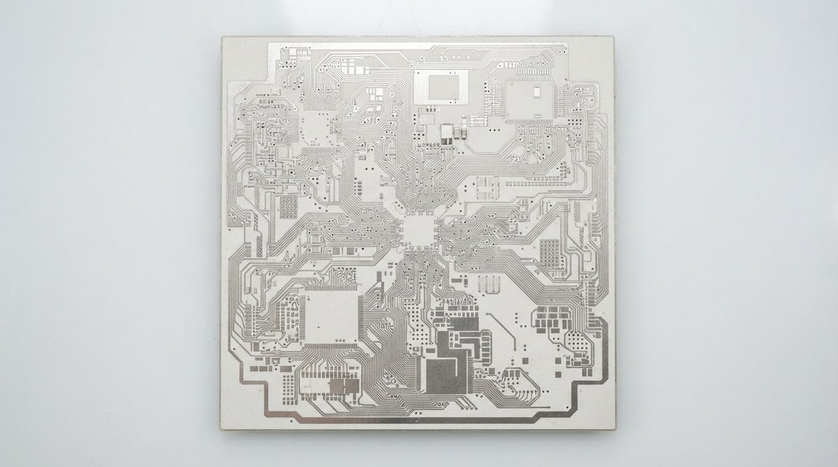
Many ceramic PCB processes — DPC (Direct Plated Copper), thin-film sputtering, and DBC (Direct Bonded Copper) — start with a substrate that has already been sintered by the material supplier. The PCB fabricator buys a fully dense, dimensionally stable blank and applies metallization afterward. No shrinkage compensation is needed in the circuit artwork, and fine features down to 20–50 µm line/space are achievable.
This is why thin-film metallization capabilities and thick-film layout guidelines assume a fixed substrate dimension. The sintering was someone else’s problem — but the substrate’s fired quality (density, surface roughness, camber) still matters enormously. A substrate with 94 % density instead of 96 % will have open surface pores that trap seed-layer material during sputtered seed layer deposition, causing adhesion defects.
How Sintering Quality Affects Downstream Processing
Under-fired substrates cause a cascade of problems. Surface porosity traps plating chemistry, leading to blistering during thermal cycling. Low density reduces flexural strength below the 350–400 MPa typical of well-sintered 96 % alumina (per ASTM C1161 four-point bend), increasing breakage during depaneling. Residual binder carbon degrades dielectric strength below the expected 14–16 kV/mm (per IEC 60672).
Over-firing is also harmful. Excessive grain growth (grains > 10 µm) reduces strength by the Hall-Petch relationship and can increase surface roughness, degrading thin-film design rule compliance. For AlN, over-firing drives yttria-aluminate phases to the surface, creating a glassy layer that impedes metallization adhesion unless removed by lapping.
When Ceramic Firing Sintering Is Not Your Concern
If you are specifying a DPC, DBC, or AMB ceramic PCB, you are buying pre-sintered substrates. Your focus should be on incoming substrate inspection — density, camber (< 0.1 mm over 100 mm is a common spec), and surface finish (Ra < 0.4 µm for thin-film). You do not need to specify a firing profile, but you should specify the substrate grade (e.g., Al₂O₃ 96 % vs. 99.6 %) because each grade has a different sintering history that determines its final properties.
For standard FR-4 or metal-core PCB applications operating below 130 °C with no need for high dielectric strength or CTE matching to semiconductor die, ceramic firing sintering knowledge is irrelevant — and the cost premium of ceramic is unjustified. Ceramic substrates make sense when thermal, frequency, or environmental demands exceed organic laminate limits. For the thermal boundaries of fired ceramic substrates, see ceramic PCB temperature limits.
Frequently Asked Questions
Does sintering change the chemical composition of the ceramic?
No. Sintering is a physical densification process — no chemical reaction changes the base ceramic phase. However, sintering aids (glass frit in LTCC, yttria in AlN) form secondary phases at grain boundaries that affect thermal and dielectric properties. The primary Al₂O₃ or AlN phase remains chemically unchanged.
Can you re-fire a ceramic substrate to fix defects?
Generally no. Once a substrate is fully sintered, re-firing provides negligible additional densification and risks warpage, grain growth, and damage to any existing metallization. Defective fired substrates are scrapped, not reworked.
Why can’t copper be co-fired in HTCC?
Copper melts at 1 085 °C, far below the 1 500–1 600 °C HTCC firing range. It would liquify and diffuse into the ceramic body, destroying both the conductor and the substrate. HTCC uses tungsten or molybdenum, which remain solid above 2 600 °C. For copper on ceramic, post-fire processes like electroplated copper buildup or DBC are used instead.
What is “zero-shrinkage” LTCC?
Zero-shrinkage LTCC constrains X-Y shrinkage to near zero by applying sacrificial layers or mechanical pressure during firing, forcing all shrinkage into the Z-axis. This improves positional accuracy to ± 0.1 % or better, at the cost of added process complexity and higher Z-axis shrinkage (up to 40 %). Ferro and DuPont both offer tape systems designed for this approach.
How do I verify that a substrate is properly sintered?
Measure density via the Archimedes method (ASTM C373) and compare to the supplier’s datasheet. Flexural strength testing (ASTM C1161) and surface roughness measurement (profilometry, Ra) are secondary checks. A density below 95 % of theoretical for the specified grade is cause for rejection.
Does firing atmosphere matter for alumina?
For pure alumina without co-fired metallization, air firing is standard and sufficient. When tungsten or molybdenum conductors are co-fired (HTCC), a reducing atmosphere (H₂/N₂ mix) is mandatory to prevent conductor oxidation. The atmosphere choice is driven by the metal, not the ceramic.