Ceramic firing sintering capability defines the dimensional accuracy, material density, and electrical performance of every ceramic PCB substrate. The process window—peak temperature, hold time, atmosphere, and heating rate—determines final shrinkage, grain structure, and whether metallization survives the furnace. Understanding ceramic firing sintering capability is essential for making sound design and sourcing decisions, and this page lists the tolerances and limits you need.
Key Takeaways
- HTCC alumina (Al₂O₃ 96%) fires at 1 500–1 600 °C with linear shrinkage of 15–20%, controlled to ±0.3–0.5% of nominal.
- LTCC glass-ceramic tapes fire at 850–900 °C, enabling co-firing with silver and gold conductors but not copper above ~6 µm without atmosphere control.
- Post-fire substrates (DPC, DBC, AMB) skip the shrinkage problem entirely because the ceramic is already sintered before metallization.
- Shrinkage mismatch is the single largest source of positional error in co-fired ceramic; it compounds with layer count.
- Firing atmosphere (air, N₂, N₂/H₂) constrains your metallization metal choices—tungsten and molybdenum for HTCC in H₂, silver and gold for LTCC in air.
What Happens During Ceramic Firing and Sintering
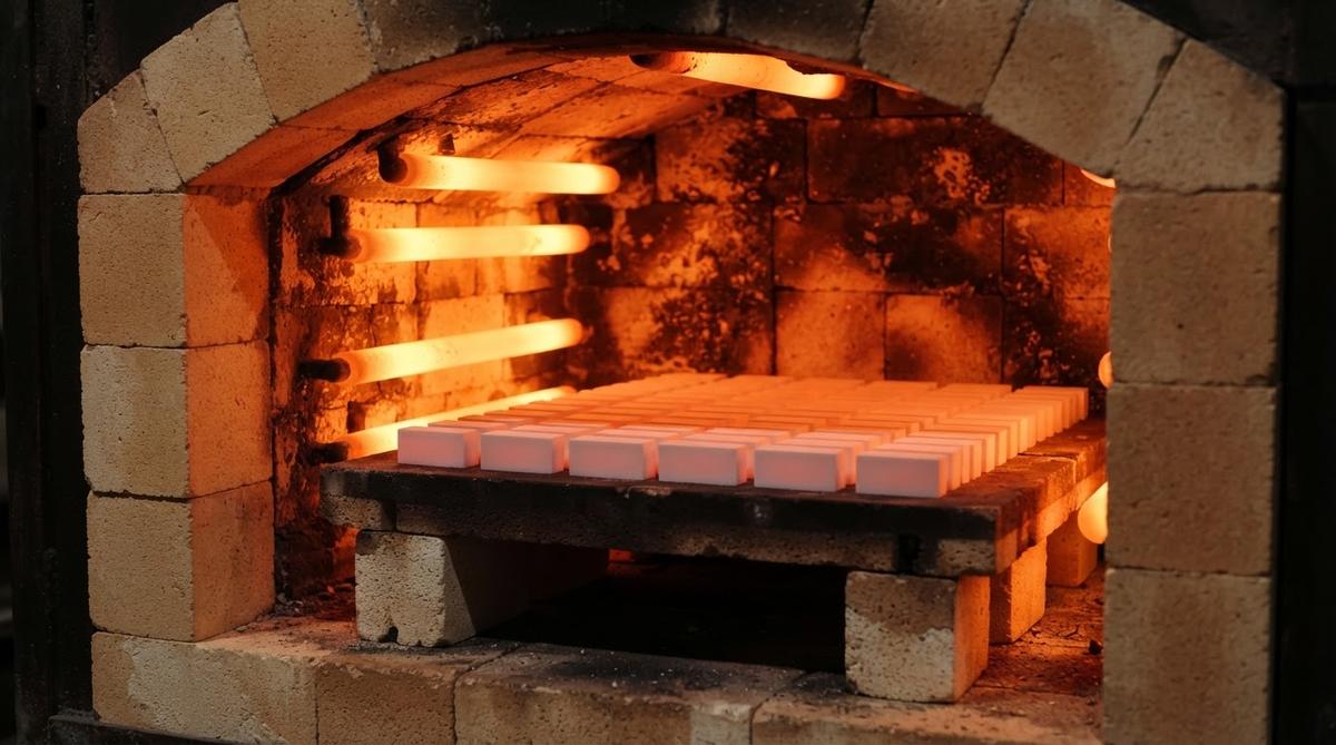
Sintering is a solid-state diffusion process. Green-state ceramic particles bond at temperatures below their melting point, eliminating porosity and shrinking the part. The final density target for structural substrates is ≥95% of theoretical density; for high-frequency or high-thermal-conductivity grades, ≥98% is typical. Grain growth during the hold period affects both mechanical strength and dielectric loss, so the profile is tightly controlled.
A standard HTCC alumina firing profile ramps at 2–5 °C/min through binder burnout (300–600 °C), then at 5–10 °C/min to peak, holds for 1–4 hours, and cools at a controlled rate to avoid thermal shock cracking. Faster ramps risk delamination in multilayer ceramic builds because trapped organics generate internal pressure.
Ceramic Firing Sintering Capability by Material and Process
| Process / Material | Peak Temperature | Atmosphere | Co-fired Metals | Linear Shrinkage |
|---|---|---|---|---|
| HTCC – Al₂O₃ 96% | 1 500–1 600 °C | H₂ / N₂-H₂ | W, Mo, Mo-Mn | 15–20% |
| HTCC – AlN | 1 750–1 900 °C | N₂ | W | 17–20% |
| LTCC – glass-ceramic | 850–900 °C | Air | Ag, Au, Ag-Pd | 12–16% |
| LTCC – constrained | 850–900 °C | Air | Ag, Au | ~0% X-Y (Z only) |
| Post-fire (DPC, DBC, AMB) | N/A (substrate pre-sintered) | — | Cu (bonded after) | 0% |
Typical values for commercially available materials, for comparison only. Confirm against the datasheet for your specific grade.
The table highlights a fundamental trade-off in ceramic firing sintering capability: co-fired processes (HTCC, LTCC) embed conductors inside the ceramic but impose shrinkage management. Post-fire processes like thick-film metallization or DBC apply metal to an already-dimensioned substrate, so registration accuracy depends on the metallization step rather than the furnace.
Shrinkage Tolerances and Positional Accuracy
Shrinkage itself is predictable; the tolerance around that prediction is what matters for pad registration. Industry-standard HTCC achieves ±0.3–0.5% of the nominal shrinkage value on X-Y dimensions, per Kyocera and CoorsTek published datasheets. On a 100 mm part with 17% nominal shrinkage, the fired dimension targets 83 mm ±0.25–0.42 mm.
Worked Example: Via-to-Pad Misregistration in a 10-Layer HTCC
Assume a 50 mm × 50 mm fired footprint, 17% nominal shrinkage (green dimension = 60.24 mm), and ±0.3% shrinkage tolerance. Worst-case positional shift at the substrate corner:
0.003 × 60.24 mm × 0.17 = ±0.031 mm per axis from shrinkage alone. Add layer-to-layer registration (typically ±25–50 µm per lamination step) and the cumulative error at 10 layers can reach ±0.08–0.12 mm. That error budget drives minimum capture pad diameter. If your design demands ±25 µm feature placement, co-fired processes will not deliver it—use a post-fire approach with photolithography instead, such as thin-film patterning on pre-sintered substrates.
Enter your substrate dimensions, shrinkage percentage, and layer count below to estimate the temperature derating and dimensional tolerance for your specific design.
Atmosphere and Its Effect on Metallization
HTCC fires in a reducing or inert atmosphere because tungsten and molybdenum oxidize in air above 500 °C. This limits HTCC conductor choices to refractory metals, which have higher resistivity (W: ~5.5 µΩ·cm, Mo: ~5.7 µΩ·cm) than copper (1.7 µΩ·cm) or silver (1.6 µΩ·cm). If low line resistance matters more than high-temperature survival, LTCC or post-fire copper may be a better fit. Atmosphere control is a core part of ceramic firing sintering capability that directly constrains your metallization options.
LTCC fires in air, so silver and gold conductors survive. However, silver migration is a reliability concern at fine pitch under DC bias in humid environments. Gold avoids migration but costs roughly 50× more per volume. Constrained-sintering LTCC variants use sacrificial layers to limit X-Y shrinkage to near zero, improving registration at the cost of Z-axis thickness tolerance.
Post-Fire Substrates: Avoiding the Shrinkage Problem
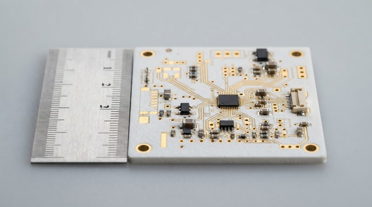
For designs that need tight dimensional control—RF filters, flip-chip interposers, high-density power modules—starting with a pre-sintered, lapped substrate eliminates firing shrinkage from the tolerance stack entirely. The substrate arrives at its final dimension; metallization is applied by sputtering (thin film), screen printing (thick film), or direct copper bonding. Registration then depends on photomask alignment (±5–10 µm for thin film) or screen alignment (±25–50 µm for thick film), not furnace behavior.
Post-fire approaches pair well with copper plating processes that build conductor thickness after patterning, giving finer line resolution than co-fired buried traces. Evaluating ceramic firing sintering capability against post-fire alternatives is the first step in choosing the right manufacturing route.
When Not to Use Co-Fired Sintering
Co-fired sintering adds cost and complexity that is not justified in every case. Skip it when:
- Single- or double-sided boards with no buried vias. A pre-sintered alumina substrate with DPC or thick-film metallization is simpler, cheaper, and more dimensionally accurate.
- Feature placement tighter than ±50 µm. Shrinkage tolerance in HTCC and LTCC cannot reliably hit this. Use thin-film lithography on a post-fire substrate.
- Copper conductors are required for low resistance. HTCC cannot co-fire copper. LTCC can co-fire copper only with nitrogen atmosphere and tight oxygen partial-pressure control, which few LTCC foundries offer at production scale.
- Prototype volumes where NRE for tape casting and screen sets is prohibitive. A laser-scribed panel of post-fire substrates reaches the bench faster.
Frequently Asked Questions
What causes warpage during ceramic firing?
Warpage results from non-uniform shrinkage, usually caused by uneven binder distribution, asymmetric metallization loading, or temperature gradients in the kiln. Typical flatness spec for a fired 96% alumina substrate is ≤0.1 mm per 25 mm, per CoorsTek ADS-996 datasheet. Symmetrical layer stackups and slow ramp rates reduce warpage.
Can you re-fire a ceramic substrate to fix a defect?
Generally no. Re-firing risks additional grain growth, conductor diffusion, and further shrinkage. Thick-film conductors on post-fire substrates can sometimes be stripped and re-printed, but co-fired parts with embedded metallization cannot be reworked after sintering.
Does sintering temperature affect dielectric constant?
Yes. Higher sintering temperatures and longer holds increase density and reduce porosity, which raises the effective dielectric constant. For 96% alumina, εr ranges from 9.0 to 9.8 at 1 MHz depending on final density (per ASTM D150). A 2% density change can shift εr by 0.3–0.5, enough to detune a filter at GHz frequencies.
What is the maximum substrate size that can be co-fired?
Practical limits for HTCC are roughly 150 mm × 150 mm after firing, constrained by kiln uniformity and shrinkage control. LTCC panels can reach 200 mm × 200 mm in production. Larger parts are possible but require tighter process control and accept wider dimensional tolerances.
How does firing affect via integrity?
Vias filled with tungsten or molybdenum paste shrink with the ceramic. Mismatch in shrinkage rate between the metal fill and the ceramic body can cause via cracking or delamination. Paste formulation is matched to the ceramic’s shrinkage curve. For post-fire substrates, vias are drilled and filled after sintering, avoiding this failure mode—see via filling capabilities for those tolerances.
Next Step
If you are deciding between a co-fired and post-fire approach for your next ceramic board, gather your feature-placement tolerance, conductor resistivity requirement, and layer count. Those three parameters usually resolve the choice. For a quote on either process, submit your files through the ceramic PCB manufacturing overview or request pricing directly.